Here’s an example of using a 1MHz by dividing FXOSC by 8, and supplying a 1MHz clock for
peripheral set 1, 100 kHz for peripheral set 2, 250 kHz for peripheral set 3.
You can notice that divider configuration register is made of three 8 bit register instead of one
32bit. See MPC5604B_M27V.h to see how registers are laid out for different modules.
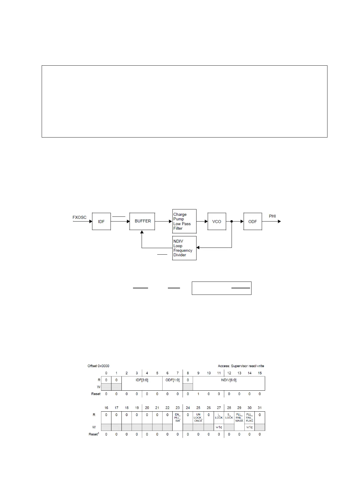
Use of FMPLL allows generating high speed clock by using FXOSC. Its block diagram is on the
figure below.
Figure 16 : FMPLL Block Diagram (Reference Manual Rev8 – Fig. 6-6)
When the PLL is locked we have
= PHI
, so PHI = FXOSC
.
.This module has the
following constraints:
FXOSC
[
4MHz, 16MHz
]
VCO
[
256MHz, 512MHz
]
NDIV
[
32, 96
]
IDF
[
1,15
]
ODF {2,4,8,16}
PHI 64MHz
After carefully choosing values for NDIV, IDF and ODF (using a spread sheet for instance), you
can use the control register of FMPLL module to implement it.
Figure 17 : FMPLL Control Register (Reference Manual Rev8 – Fig. 6-7)
CGM.FXOSC_CTL.R = 0x00800700; /* keep reset settings but divide by 8 */
...
/* Here insert code that configures a user mode’s system clock with divided
xtal fast oscillator, you can check it with CGM.SC_SS.R read only register */
CGM.SC_DC[0].R = 0x00; /* no division for peripheral set 1 */
CGM.SC_DC[1].R = 0x89; /* divide by 10 for peripheral set 2 */
CGM.SC_DC[2].R = 0x83; /* divide by 4 for peripheral set 3 */
/* Here insert code that makes the mode transition towards the user mode with