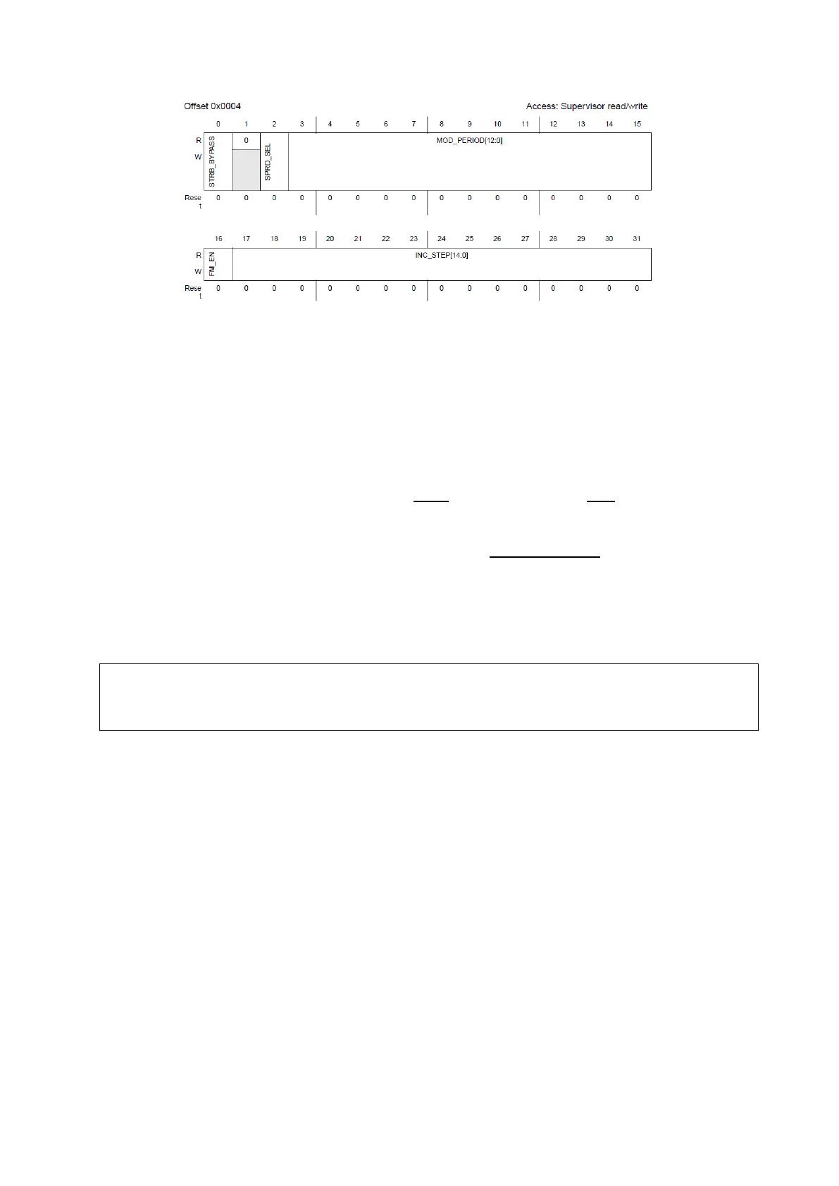
Figure 19 : FMPLL Modulation Register (Reference Manual Rev8 – Fig. 6-8)
Different fields of this register are defined as:
STRB_BYPASS: Strobe bypass; when this bit is set to ‘0’, it allows to change other fields
while FM is not enabled, but if it is set to ‘1’, other fields has to be static while FMPLL is
powered on,
SPRD_SEL: spread selection, if it is ‘0’, the FM is centre spread, if it is ‘1’, the FM is down
spread (see Figure 18),
MOD_PERIOD[12:0]: binary value of
, where
= .
and
is the
modulation frequency,
INC_STEP[14:0]: binary value of =
××
××
,
FM_EN: enable FM by writing ‘1’.
MOD_PERIOD and INC_STEP have to be calculated using selected values of
and in order
to respect the following limitation: _× _
(
2
1
)
.
Recommended modulation depths are ±0.25% to±4% for center spread and 0.5% to8% for
down spread.
A device initialisation procedure
We’ve seen different steps to follow for initialising the microcontroller, we can now write a
generic initialisation function that could be used for a lot of embedded applications.
The structure of the code will remain the same for most of the embedded applications:
Enable modes that may be used.
Make the clock configuration.
Mode configuration.
Peripheral configuration.
Transition towards a user mode.
CGM.FMPLL_MR.B.MOD_PERIOD = 20; /* fmod=50kHz */
CGM.FMPLL_MR.B.INC_STEP = 29; /* md = 0.1% */
CGM.FMPLL_MR.B.FM_EN = 1; /* enable FM */