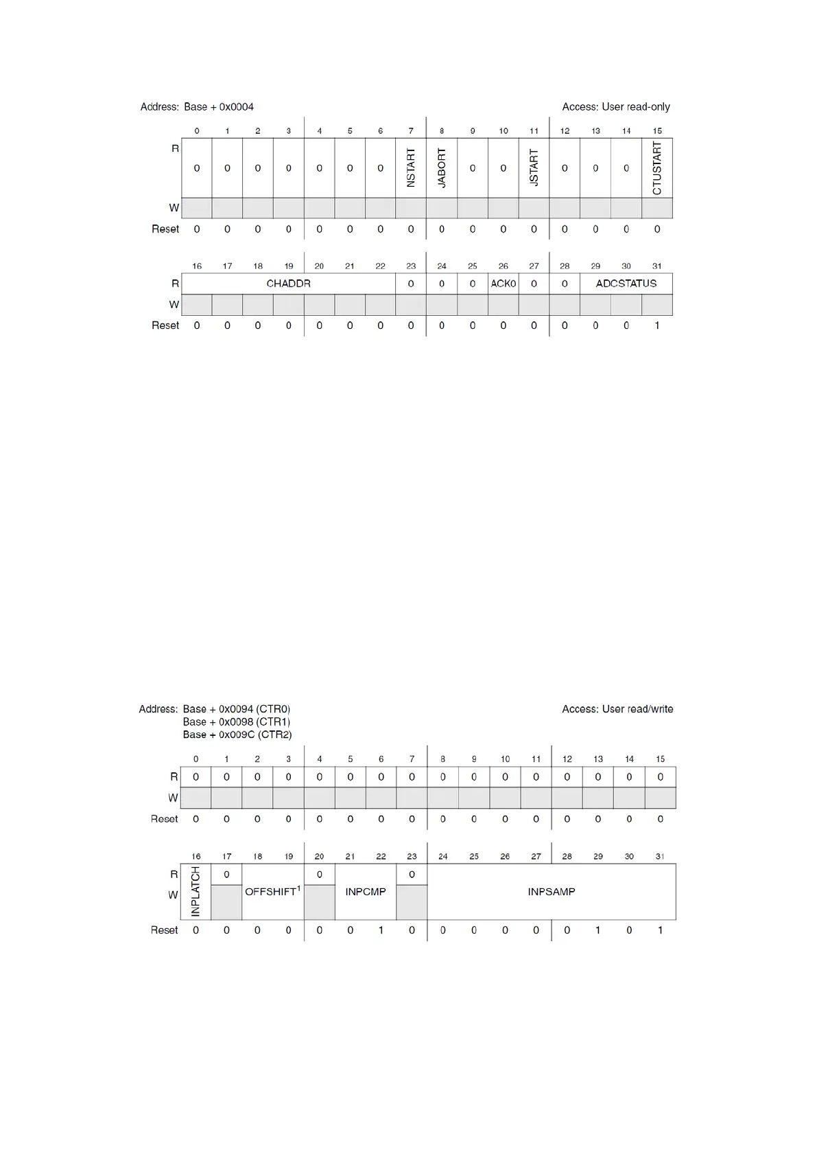
Figure 72 : Main Status Register (R.M. Rev8 – Fig. 25-9)
The Main Status Register (MSR) is a read-only register allowing the access the current status of
the ADC module: NSTART, JSTART, CTUSTART respectively indicate whether a conversion of
normal, injected or CTU modes is ongoing, CHADDR indicates current conversion channel
address, JABORT signals if an injected conversion is aborted. ADCSTATUS field’s values depend
on ADC’s status: idle (000), power-down (001), wait state (010), sample (100), conversion
(110).
The Decode Signal Delay Register (DSDR) allows to put a delay between the external decode
signals and the sampling phase. It is useful for taking in account the settling time of the external
multiplexers. It has a 8-bit field called DSD and it introduces DSD/2 ADC clock delays.
The Power-Down Exit Delay Register (PDEDR) delays the beginning of a conversion after leaving
the power-down mode, to allow the ADC power supply to stabilise. It has an 8-bit field named
PDED and it introduces PDED ADC clock delays.
Figure 73 : Conversion Timing Register (R.M. Rev8 – Fig. 25-26)
The Conversion Timing Registers (CTR[0...2]) are used for configuring the timing of different
phases in the ADC process, for the three types of inputs(respectively, precision, standard,
external standard). See the previous sections on conversion timing for more information about