D3-DU 3xx/A, /B Connections and wiring
Project engineering manual V1.09
57
© KEBA 2021
KEBA does not perform any tests for the correct functionality of operating
devices from third-party manufacturers.
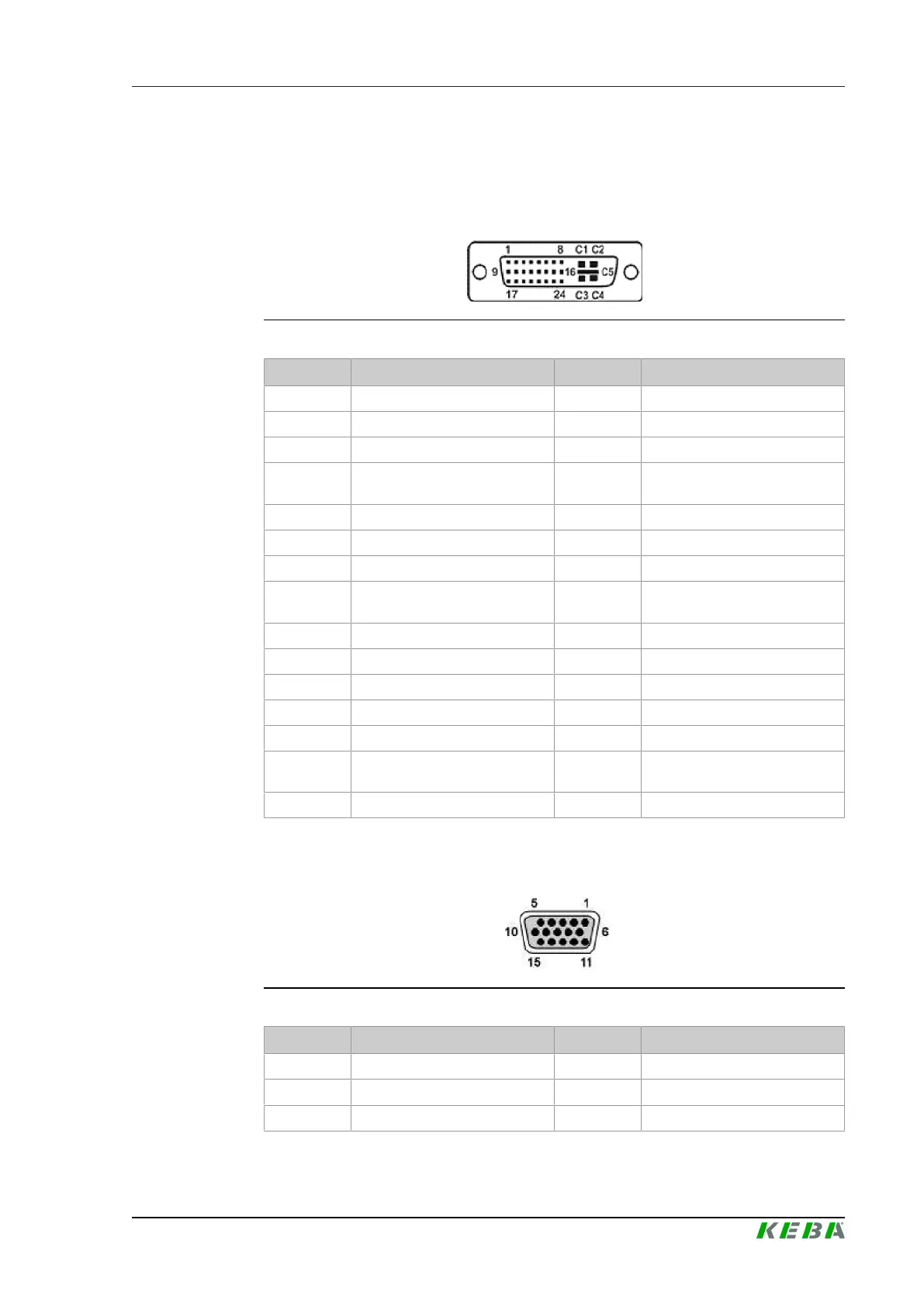
6.4.1 Pin assignment
Fig.6-29: Pin assignment DVI socket
Pin no. Designation Pin no. Designation
1 TDMS-Data 2- 2 TDMS-Data 2+
3 Shielding TDMS-Data 2,4 4 TDMS-Data 4-
5 TDMS-Data 4+ 6 DDC clock (SDC)
7 DDC clock (SDA) 8
Analog: V-Sync to RS485 TX/
RX
9 TDMS-Data 1- 10 TDMS-Data 1+
11 Shielding TDMS-Data 1,3 12 TDMS-Data 3-
13 TDMS-Data 3+ 14 +5 V
15 Ground for +5 V 16
Hotplug-Detect, enable RS485
Transceiver
17 TDMS-Data 0- 18 TDMS-Data 0+
19 Shielding TDMS 0,5 20 TDMS-Data 5-
21 TDMS-Data 5+ 22 Shielding TDMS-clock
23 TDMS-clock+ 24 TDMS-CLK-
C1 n.c. C2 n.c.
C3 n.c. C4
Analog: H-Sync- to RS485 TX/
RX-
C5 Analog: Ground → GND
6.4.2 KEBA operating panel pin assignment
Fig.6-30: Pin assignment D sub socket
Pin no. Designation Pin no. Designation
1 CLK+ (Pair 1) 2 CLK- (Pair 1)
3 +5 V 4 RS-485+ (Pair 2)
5 RS-485- (Pair 2) 6 DATA0+ (Pair 3)
 Loading...