2G0947 - 31JAN08 7-1
Section 7: Functional Diagrams
A B C D E F G H J K L M N P Q R S T U V W X Y ZAA
T U V W X Y Z AAA B C D E F G H J K L M N P Q R S
16
15
14
13
12
11
10
9
8
7
6
5
4
3
2
1
16
15
14
13
12
11
10
9
8
7
6
5
4
3
2
1
2008 January Rev. A 2G0849
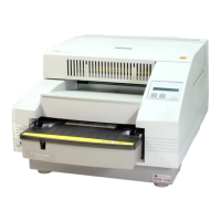
Kodak DryView 5800 LASER IMAGER - System Functional Block / Wiring Diagram - Sheet 1 of 4
Imaging Assembly
1
2
3
J1/P1
1
2
3
4
5
6
7
8
DC to DC
Conv./
Reg
Splitting
Lens
2% Beam Sample
Filter
+5V(A)
HF RF
OSC
400
MHz
Trans
Drive
RF
Comp
Opt.
SW /
FET
Enable
Enable
Gain
U1 Buf
0-2V
Feed
Back
Laser Driver Board
-
5V(A)
+24V
+5V(A)
+5V(A)
-
5V(A)
-5V(A)
A
A
Laser Beam to
Polygon Mirror
Laser
Diode
JP1
A
DICOM Raster Engine (DRE)
Motherboard
M10
Polygon
Spinner
Motor
Polygon
Mirror
1
2
3
4
5
1
2
3
4
5
Polygon
Sensor
Network Cable
12 VDC Power
Power
Data
Service
Network
Connector
RJ45
Monitor
Connector
(Not Used)
USB
Connectors (2)
From
Modalities
J1
1
2
3
4
J2
1
2
3
4
P1/J1
Data
Clock
I
2
C
Reset
Circuit
NVRAM
<
<
<
<
OSC
Freq
Div.
Micro
Proc.
Amp
Amp
A to D
Conv
16 MHz
Happy
S11
S10
<
<
+5V
+5V
+5V
+5V
+5V
+5V
+3.3V
D2
D
ensity
Fiducial
Densitometer
Lightsource
Board (DLB)
Densitometer
Control Board (DCB)
Film Path Micro (FPM) Board
J7
J10
1
2
3
4
5
6
7
8
9
10
11
12
13
14
DC Power and
I
2
C
DC Power and
I
2
C
<
<
Laser Beam
from Laser Diode
24 V DC Power Supply
See sheet 3
See sheet 3
To Focusing
Lenses
J11
J20
24 VDC Power
>
>
For Service Use
1
2
3
4
1
2
3
4
5
6
7
8
1
2
3
4
5
6
7
8
A
Start of Page (SOP)
Sensor
S8
Power and
I
2
C
1
2
3
4
Hard Drive
1
2
3
4
5
6
7
8
9
USB1 (Header)
[Not Functional]
Rear
RJ45
Connector
Network Cable
RJ 45
<
{
Output - Sensor
Blocked = LOW
+5V
Optics Module
Optics Module
J7
J2
1
2
3
J3
1
2
3
4
5
6
7
8
9
J1
J6
+5V
Config
Flash
Mem
Micro
Processor
and USB
Controller
FPGA
Laser
Drive
(Analog)
Pixel
DAC
Flash
Memory
+5V
+5V(A)
NU
+5V
Data Path Board (DPB)
+5V(A)
<
SDRAM
Image
Memory
+5V(USB)
1
2
3
4
5
6
7
8
Serial
DS4 DS6 DS5
Laser Enable
Micro Processor
Boot Code
I
2
C
<
<
<
<
Pixel
Data
Clock
Data
<
SOP
FPGA
Program
Interface
Gain and
Offset
DACs
-5V(A)
+3.3V
DS3
DS2
+3.3V
Reset
Switch
LASER +24V
Laser OFF
U16
U11
- USB
+USB
PolyIndex
I
2
C
Buffer
1
2
3
4
5
6
7
8
9
10
11
12
13
14
15
16
SOP
+5V
+3.3V
+3.3V
Micro
Processor
Enable Laser
U18
SOS
EOS
SCL SOS
SDA SOS
SCA EOS
SCL EOS
1
2
3
4
5
6
7
8
9
10
BPM Reset
BPM Reset
(Stores 1 image)
SOS
EOS
J5
< >
< >
Voltage
Regulators
NU
+5 V
+1.2 V
+3.3 V
+5 V (A)
-5 V (A)
NOTE: 5V(A) = 5V for analog circuits
A
NU
A to D
Conv.
<
Data
Clock
<
NU
1
2
3
4
5
6
7
8
9
10
11
12
13
14
LASER +24V
+5V
11
12
NU
NU
Poly Start
Poly L ock
Polygon Clock
<
<
<
<
+5v(A)
<
J1A
1
2
3
4
5
NU
Not
Used
USB
Connector
-5v(A)
SOP
Start of
Scan (SOS)
Board
End of
Scan (EOS)
Board
M7
Exposure Transport Motor
and Circuit Board
(See Sheet 3)
Keyboard/Mouse
Connector
(Not Used)
Filter
Plate
USB
1
2
3
4
5
6
7
8
9
USB2
(Header)

 Loading...

