NVIDIA Jetson Nano DG-09502-001_v2.1 | 7
Chapter 3. Developer Kit Feature
Considerations
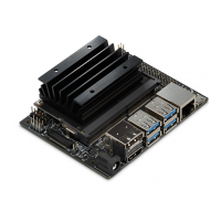
The Jetson Nano Developer Kit Carrier Board design files are provided as a reference design.
This chapter describes details necessary for designers to know to replicate certain features if
desired. In addition, aspects of the design that are specific to the NVIDIA Developer Kit usage
but not useful or supported on a custom carrier board are also identified.
Most of the features implemented on the Jetson Nano Developer Kit carrier board design can
be duplicated by copying the connections from the P3449 carrier board reference design. The
Some features have aspects that would require additional information as listed
USB SuperSpeed Hub
Power over Ethernet (PoE)
TI TXB0108 level shifters
ID EEPROM (Not to be copied from reference design)
3.1 USB SuperSpeed Hub
The USB SS hub design uses a Realtek RTS5411S device. The hub device has been customized
using internal fuses with the Realtek tool. A design intending to duplicate the DevKit hub
implementation should customize the hub as follows:
Power enables (DPS1/2/3/4_PWR) set to be active high
Charging feature disabled
SSC valid
3.2 Power Over Ethernet (PoE)
The P3449 carrier board includes a 4-pin Power over Ethernet (PoE) header (J38) which brings
out the VC power pins of the Ethernet connector. In order to use this alternate PoE power
mechanism to power the carrier board, the design would require a power converter to take the
high voltage PoE supply (38V-60V) and convert it to the correct voltage for the custom carrier
board. This could be the 5V that the Jetson Nano DevKit uses, or a different voltage depending
on the design of the custom carrier board.

 Loading...