USB and PCI Express
NVIDIA Jetson Nano DG-09502-001_v2.1 | 22
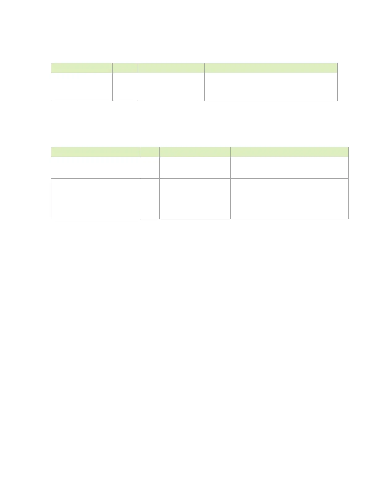
Table 6-7. Miscellaneous USB 2.0 Signal Connections
Module Pin Name Type Termination Description
GPIO00 A 5V to 1.8V level shifter USB0 VBUS Enable: Connect to VBUS pin of USB
connector receiving USB0_+/– interface through level
shifter. Also connects to VBUS power supply if host mode
supported.
Table 6-8. Tegra USB 3.0 Signal Connections
Module Pin Name Type Termination Description
USBSS_TX_N/P (USB 3.0 Port #0) DIFF
Out
Series 0.1uF caps. ESD
Protection near connector if
required.
USB 3.0 Differential Transmit Data Pairs: Connect
to USB 3.0 connectors, hubs or other devices on
the PCB.
USBSS_RX_N/P (USB 3.0 Port #0)
DIFF
In
If routed directly to a
peripheral on the board, AC
caps are needed for the
peripheral TX lines. ESD
protection near connector if
required.
USB 3.0 Differential Receive Data Pairs: Connect
to USB 3.0 connectors, hubs or other devices on
the PCB.
6.2 PCIe
NVIDIA
®
Tegra
®
contains a PCIe controller that brings one interface up to four lanes to the
module pins for use on the carrier board. A second single-lane PCIe interface is used on-
module for Ethernet.

 Loading...


