Miscellaneous Interfaces
NVIDIA Jetson Nano DG-09502-001_v2.1 | 63
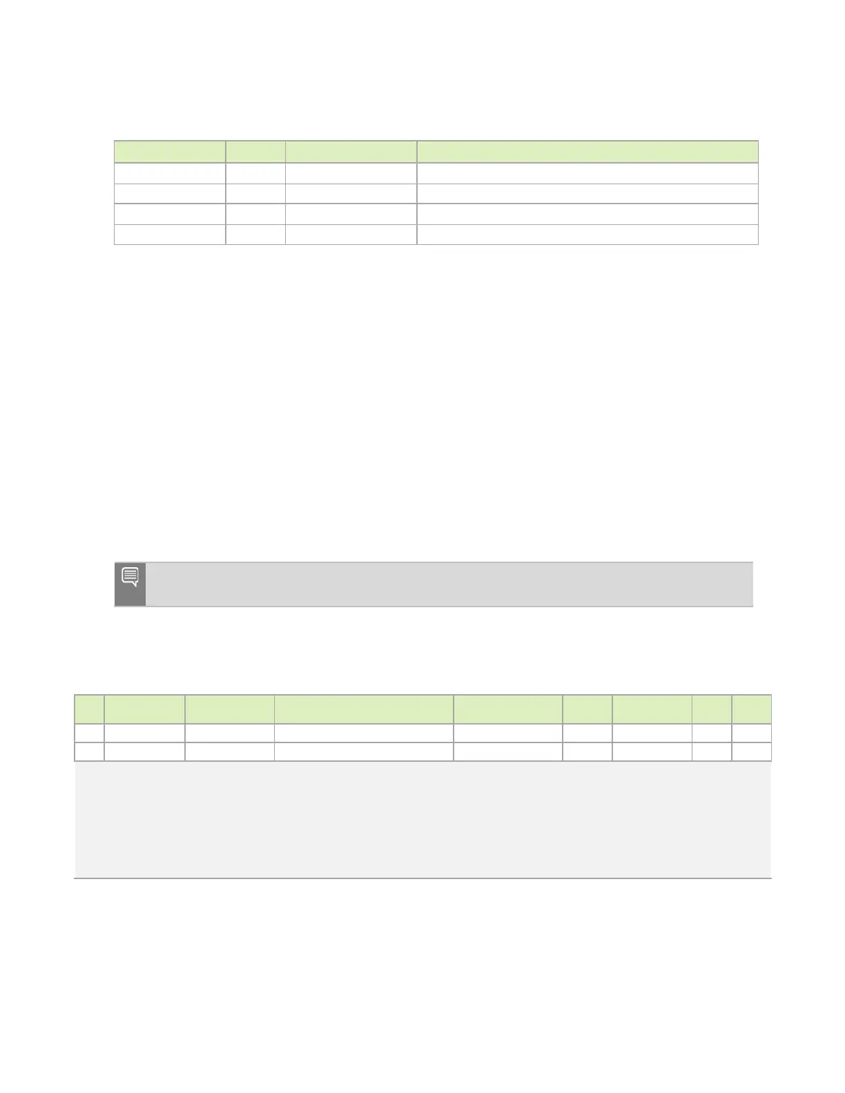
Table 11-7. UART Signal Connections
Ball Name Type Termination Description
UART[2:0]_TXD O UART Transmit: Connect to peripheral RXD pin of device
UART[2:0]_RXD I UART Receive: Connect to peripheral TXD pin of device
UART[1:0]_CTS* I UART Clear to Send: Connect to peripheral RTS pin of device
UART[1:0]_RTS* O UART Request to Send: Connect to peripheral CTS pin of device
11.4 Fan
Jetson Nano provides PWM and Tachometer functionality for controlling a fan as part of the
thermal solution. Information on the PWM and Tachometer pins/functions can be found in the
following locations:
Jetson Nano Module Pin Mux:
• This is used to configure GPIO14 (PWM) for FAN_PWM and GPIO08 (SDMMC_CD) for
FAN_TACH. The pin used for FAN_PWM is configured as PM3_PWM3. The pin used for
FAN_TACH is configured as a GPIO.
Tegra X1 (SoC) Technical Reference Manual (TRM):
• Functional descriptions and related registers can be found in the TRM for the
FAN_PWM (PWM chapter).
Note: For Table 11-8 and Table 11-9, in the Direction column, Output is from Jetson Nano. Input
is to Jetson Nano. Bidir is for bidirectional signals.
Table 11-8. Jetson Nano Fan Pin Description
Pin # Module Pin Name Tegra X1 Signal Usage/Description
Usage on NVIDIA DevKit
Direction Pin Type
Power-on
230 GPIO14 GPIO_PE7 Fan PWM Fan Output CMOS – 1.8V ST pd
208 GPIO08 GPIO_PX2 Fan tachometer Fan Input CMOS – 1.8V ST pd
Notes:
1. In the Type/Dir column, Output is from Jetson Nano. Input is to Jetson Nano. Bidir is for Bidirectional signals.
2. The directions for GPIO14 and GPIO08 are true when used for those functions. Otherwise as GPIOs, the directions are bidirectional.
3. The MPIO Pad Codes are described in the
Tegra X1 SoC Technical Reference Manual
“Multi-Purpose I/O Pins and Pin Multiplexing
(PinMux)” section for details.
4. The Power-on Reset State column indicates the pin state when reset is active and when it is deactivated before any changes are made by
software. “z” is tristate, pu/pd indicates internal weak pull-up/down resistor is enabled, 1/0 indicates actively driven high/low.

 Loading...


