Miscellaneous Interfaces
NVIDIA Jetson Nano DG-09502-001_v2.1 | 64
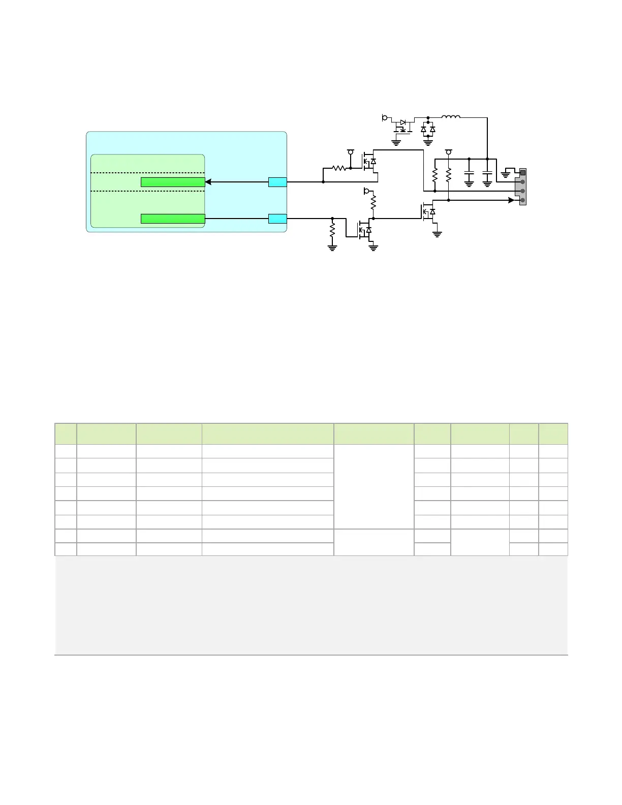
Figure 11-6. Jetson Nano Fan Connections
VDD_5V_IN
G
S
D
1
2
3
4
G
S
D
1kΩ
10 k
Ω
10uF
Fan
Header
Jetson
Tegra X1 – Fan
GPIO _PE7
DMIC
FAN_TACH
FAN_PWM
GPIO _PZ2
230
208
SYS
10 0k Ω
GP IO 08
GP IO 14
VDD_5V_IN
G
S
D
10 kΩ
10 kΩ
VDD_1V8
G
S D
0.1uF
BAT54 C
SM23 09
PSAC
-TRG
DMN2 6
DO UFB4
DMN2 6
DO UFB4
DMN2 6
DO UFB4
10 0u H
VDD_5V_IN
11.5 Debug
Jetson Nano supports JTAG and a UART for debugging purposes. JTAG is not brought to the
module pins, however, but to test points on the module. The UART intended for debug is
UART1 with is routed to a level shifter then to a 6-pin UART header on the developer kit carrier
board.
Table 11-9. Jetson Nano JTAG and Debug UART Description
Pin #
Module Pin Name
(See Note)
Tegra X1 Signal Usage/Description
Usage on NVIDIA DevKit
Carrier Board
Direction Pin Type
Code
Power-on
Reset
JTAG_GP0 JTAG_TRST_N JTAG test reset
None – JTAG not brought
to the module pins on
Jetson Nano
Input CMOS – 1.8V − −
JTAG_RTCK JTAG_RTCK JTA G ret urn clock Input CMOS – 1.8V
− −
JTAG_TCK JTAG_TCK JTA G test clock Input CMOS – 1.8V − −
JTAG_TDI JTAG_TDI JTAG test data In Input CMOS – 1.8V − −
JTAG_TDO JTAG_TDO JTAG test data Out Output CMOS – 1.8V − −
JTAG_TMS JTAG_TMS JTAG test mode select Input CMOS – 1.8V
− −
238 UART2_RXD UART1_RX UART 1 receive
Serial port
Input CMOS – 1.8V ST pd
236 UART2_TXD UART1_TX UART 1 transmit Output ST pd
Notes:
1. In the Type/Dir column, Output is from Jetson Nano. Input is to Jetson Nano. Bidir is for Bidirectional signals.
2. The direction for UART2_RXD is true when used for this function. Otherwise as a GPIO, the direction is bidirectional.
3. The MPIO Pad Codes are described in the Tegra X1 SoC Technical Reference Manual “Multi-Purpose I/O Pins and Pin Multiplexing
(PinMux)” section for details.
4. The Power-on Reset State column indicates the pin state when reset is active and when it is deactivated before any changes are made by
software. “z” is tristate, pu/pd indicates internal weak pull-up/down resistor is enabled, 1/0 indicates actively driven high/low.
5. JTAG is brought to on-module test points only.

 Loading...


