Miscellaneous Interfaces
NVIDIA Jetson Nano DG-09502-001_v2.1 | 65
11.5.1 JTAG
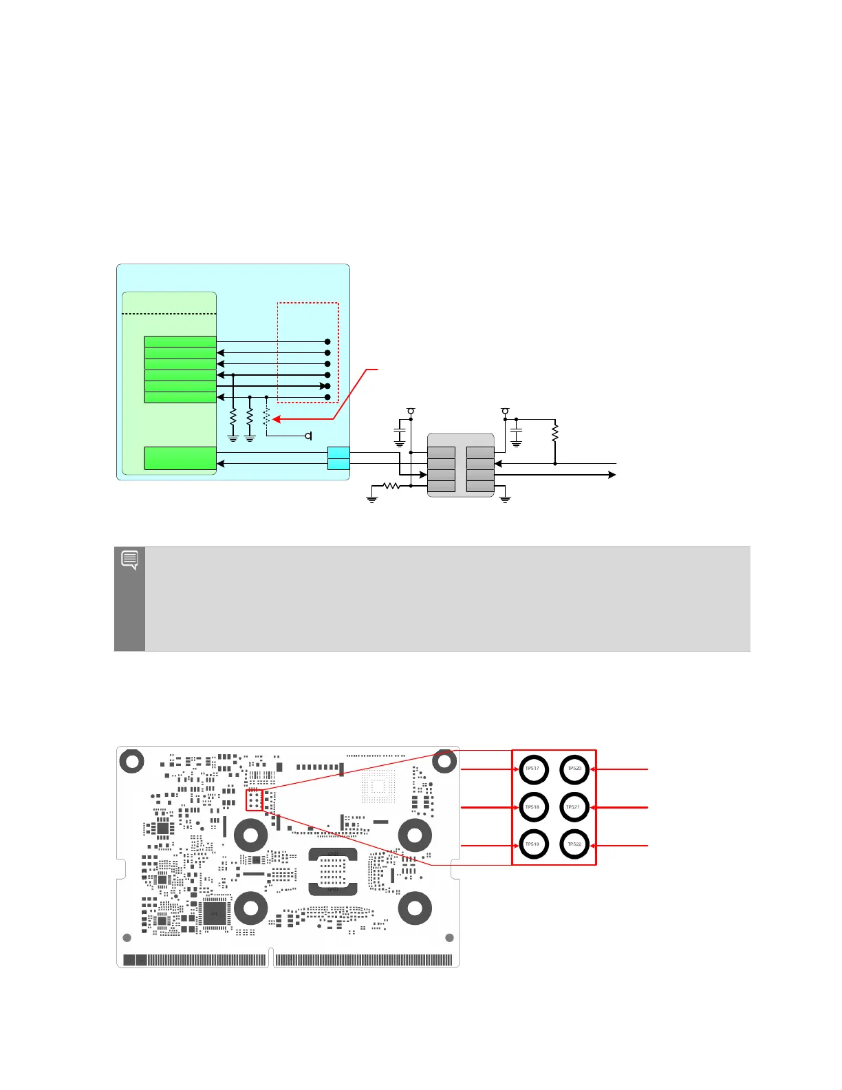
Jetson Nano provides access to JTAG via test points on the module. Figure 11-7 shows the
JTAG and debug UART connections based on the Jetson Nano Developer Kit design.
Figure 11-7. JTAG and Debug UART Connections
Jetson
Tegr a
Level Shifter
VCCBVCCA
B1A1
B2A2
GNDOE
10 0k Ω
VDD_3V 3_SYSVDD_1V8
0.1uF
0.1uF
UART 2_TXD
UART 2_RXD
236
238
UART1_TX
UART1_RX
DEBUG
10 0k Ω
RXD_LS
TXD_L S
JTAG_TRST_N
J TAG_T DI
JTAG_TMS
JTAG_TCK
JTAG_RTCK
JTAG_TDO
100kΩ
100kΩ
Op tion to al l ow JTAG _TRST to be ti e d high to
en ab le S can Mo de (Pull do wn wo uld b e remo ved ) –
Leave unconnected for normal operation or JTAG
connection to CPUs, etc.
On-Module
Test Points
10 0k Ω
R T CK
TMS
TDI
TCLK
TDO
TRST_N
VDD_1V8
Notes:
1.Pull-ups or Pull-downs are present on the UART TX and RTS lines for RAM Code strapping.
2.If level shifter is implemented, pull-up is required on the RXD line on the non-Jetson Nano side
of the level shifter. This is required to keep the input from floating and toggling when no device
is connected to the debug UART.
Figure 11-8. JTAG Test Point Detail
JTAG_TRST
JTAG_TDO
JTAG_TMS
JTAG_TCK
JTAG_TDI
JTAG_RTCK
JTAG Test Points
Jetson Nano Bottom Side View

 Loading...


