USB and PCI Express
NVIDIA Jetson Nano DG-09502-001_v2.1 | 25
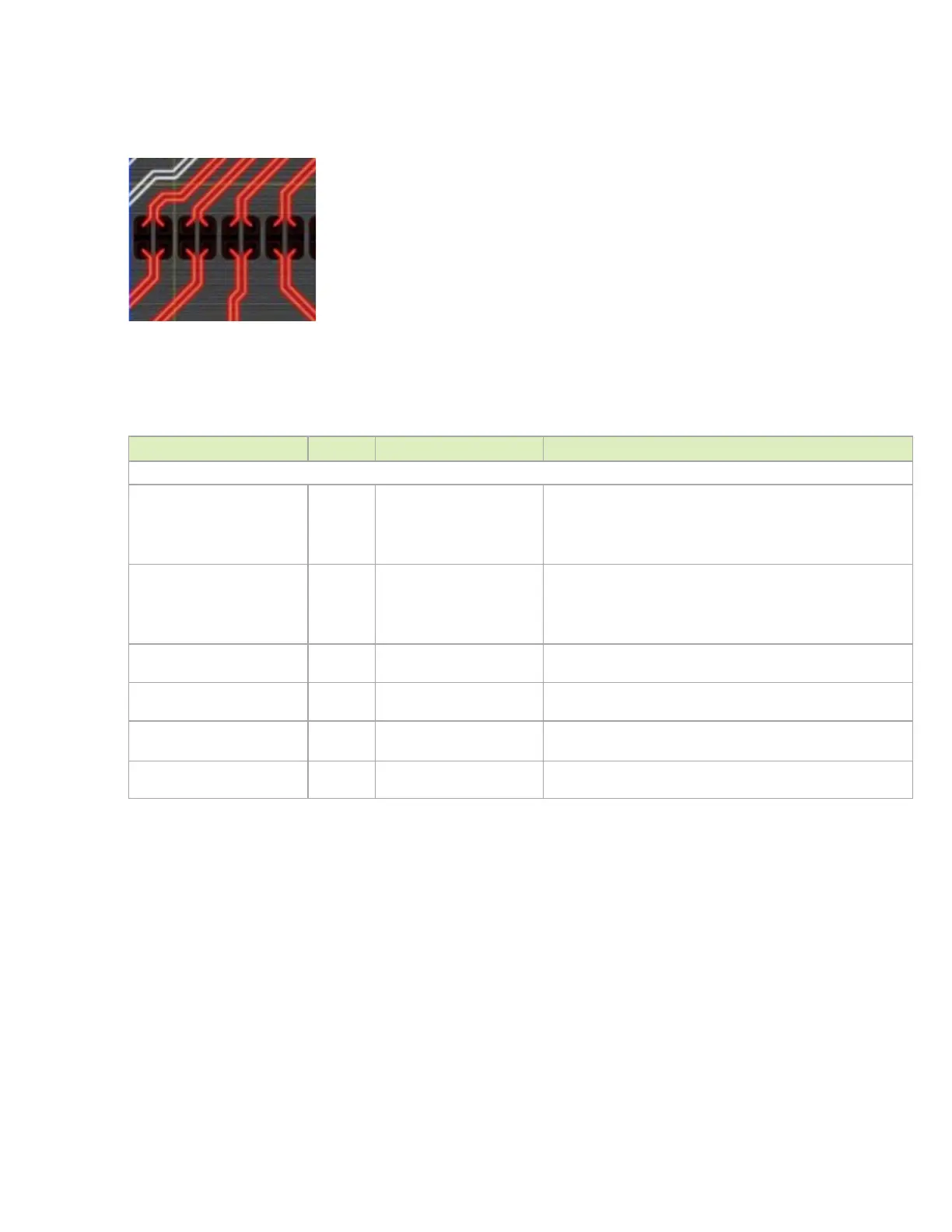
Figure 6-8. AC Cap Voiding
Table 6-10. PCIe Signal Connections
Module Pin Name Type Termination Description
PCIe Interface #0 (x4)
PCIE0_TX3_N/P (Lane 3)
PCIE0_TX2_N/P (Lane 2)
PCIE0_TX1_N/P (Lane 1)
PCIE0_TX0_N/P (Lane 0)
DIFF
OUT
Series 0.1uF Capacitor Differential Transmit Data Pairs: Connect to TX_N/P pins of
PCIe connector or
pin of PCIe device through AC cap
according to supported configuration.
PCIE0_RX3_N/P (Lane 3)
PCIE0_RX2_N/P (Lane 2)
PCIE0_RX1_N/P (Lane 1)
PCIE0_RX0_N/P (Lane 0)
DIFF IN Series 0.1uF capacitors
near Jetson Nano pins or
device if device on main
PCB.
Differential Receive Data Pairs: Connect to RX_N/P pins of PCIe
connector or
pin of PCIe device through AC cap
according to supported configuration.
PCIE0_CLK_N/P DIFF
OUT
Differential Reference Clock Output: Connect to
REFCLK_N/P pins
of PCIe device/connector
PCIE0_CLKREQ* I/O 47kΩ pull-up to
on module
PCIe Clock Request for PCIE0_CLK:
Connect to
pins
on device/connector(s)
PCIE0_RST* O 4.7kΩ pull-up to
on module
Connect to
pins on device/connector(s)
PCIE_WAKE* I 100kΩ pull-up to
on module
Connect to
pins on device or connector

 Loading...


