Display
NVIDIA Jetson Nano DG-09502-001_v2.1 | 32
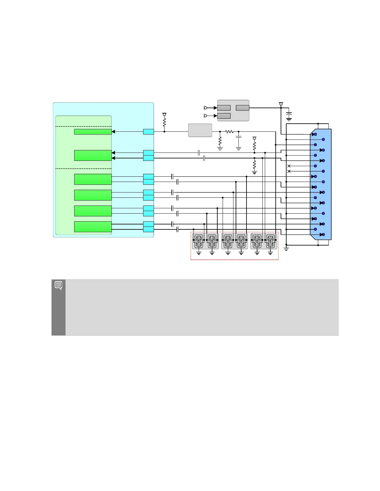
Tegra supports an eDP interface. The eDP interface can also be used for DP. DP support on
these pins does not include HDCP or Audio.
Figure 7-2. DP/eDP Connection Example on DP0 Pins
Jetson
Tegra
DP0_HPD
DP0_AUX_N
DP0_AUX_P
DP0_TXD3_N
DP0_TXD3_P
DP0_TXD2_N
DP0_TXD2_P
DP0_TXD1_N
DP0_TXD1_P
DP0_TXD0_N
DP0_TXD0_P
EDP_TXD0_N
EDP_TXD0_P
EDP_TXD1_N
EDP_TXD1_P
EDP_TXD2_N
EDP_TXD2_P
EDP_TXD3_N
EDP_TXD3_P
DP_AUX_CH0_N
DP_AUX_CH0_P
DP
eDP
DP_ HP D
0. 1uF
0. 1uF
0. 1uF
0. 1uF
0. 1uF
0. 1uF
0. 1uF
0. 1uF
0. 1uF
0. 1uF
41
39
47
45
53
51
59
57
92
90
88
10 0k Ω
VDD_3V3 _SY S
10 0k Ω
VDD_3V3 _EDP
VDD_3V3 _SY S
DP
Conn
.
PWR
PWR_RET
HPD
AUXN
GND
AUXP
CEC_DP
MODE
LA NE _3 N
GND
LA NE _3 P
LA NE _2 N
GND
LA NE _2 P
LA NE _1 N
GND
LA NE _1 P
LA NE _0 N
GND
LA NE _0 P
1
3
5
11
7
9
13
15
17
19
2
10
12
6
8
14
16
18
4
20
3V 3_IO_ PG
T PD4E 05U06
VDD_1V8
10 kΩ
10 kΩ
10 kΩ
Load Switch
EN
IN OUT
Lev el Shif te r
1.8V 3.3V
Notes:
• Level shifter required on DP0_HPD to avoid the pin from being driven when Jetson Nano is off.
The level shifter must be non-inverting (preserve the polarity of the HPD signal from the
display).
• Load Switch enable is from powergood pin of main 3.3V supply.
•
If eDP interface used for DP, note that HDCP is not supported.

 Loading...


