Miscellaneous Interfaces
NVIDIA Jetson Nano DG-09502-001_v2.1 | 66
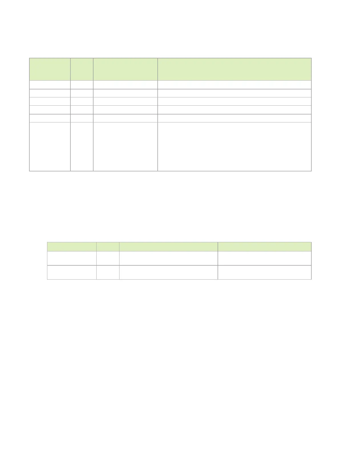
Table 11-10. JTAG Connections
Jetson Nano
Test Point
Signal Name
Type Termination Description
JTAG_TMS I JTAG Mode Select: Connect to TMS pin of connector
JTAG_TCK I 100kΩ to
JTAG Clock: Connect to TCK pin of connector
JTAG_TDO O JTAG Data Out: Connect to TDO pin of connector
JTAG_TDI I JTAG Data In: Connect to TDI pin of connector
JTAG_RTCLK I JTAG Return Clock: Connect to RTCK pin of connector
JTAG_TRST_N I 100kΩ to
JTAG Test Reset: This signal is used to select normal operation or scan
test mode operation.
• Normal operation: Leave pulldown resistor on module installed.
• Boundary Scan test mode: Connect
to
install
100kΩ resistor to VDD_1V8 and remove 100kΩ resistor to GND. Or
install strong enough resistor connected to VDD_1V8 to overcome
weak 100kΩ pulldown (1ΩΩ to 4.7kΩ).
11.5.2 Debug UART
The UART2 interface is intended to be used for debug purposes.
Table 11-11. Debug UART Connections
Module Pin Name Type Termination Description
UART2_TXD O UART #2 Transmit: Connect to RX pin of
serial device
UART2_RXD I If level shifter implemented, 100kΩ to supply
on the non-Jetson Nano side of the device.
UART #2 Receive: Connect to TX pin of
serial device

 Loading...


