Display
NVIDIA Jetson Nano DG-09502-001_v2.1 | 29
Table 7-2. Jetson Nano DSI Pin Description
Pin # Module Pin Name Tegra X1 Signal Usage/Description
Usage on NVIDIA DevKit
Carrier Board
Direction Pin Type
Code
Power-on
Reset
76 DSI_CLK_N DSI_A_CLK_N
Display, DSI clock
Not assigned
Output
MIPI D-PHY
− pd
78 DSI_CLK_P DSI_A_CLK_P −
pd
70 DSI_D0_N DSI_A_D0_N
Display, DSI data lane 0 Bidir
−
pd
72 DSI_D0_P DSI_A_D0_P − pd
82 DSI_D1_N DSI_A_D1_N
Display, DSI data lane 1 Output
− pd
84 DSI_D1_P DSI_A_D1_P −
pd
Notes:
1. In the Type/Dir column, Output is from Jetson Nano. Input is to Jetson Nano. Bidir is for Bidirectional signals.
2. The MPIO Pad Codes are described in the
Tegra X1 SoC Technical Reference Manual
“Multi-Purpose I/O Pins and Pin Multiplexing
(PinMux)” section for details.
3. The Power-on Reset State column indicates the pin state when reset is active and when it is deactivated before any changes are made by
software. “z” is tristate, pu/pd indicates internal weak pull-up/down resistor is enabled, 1/0 indicates actively driven high/low.
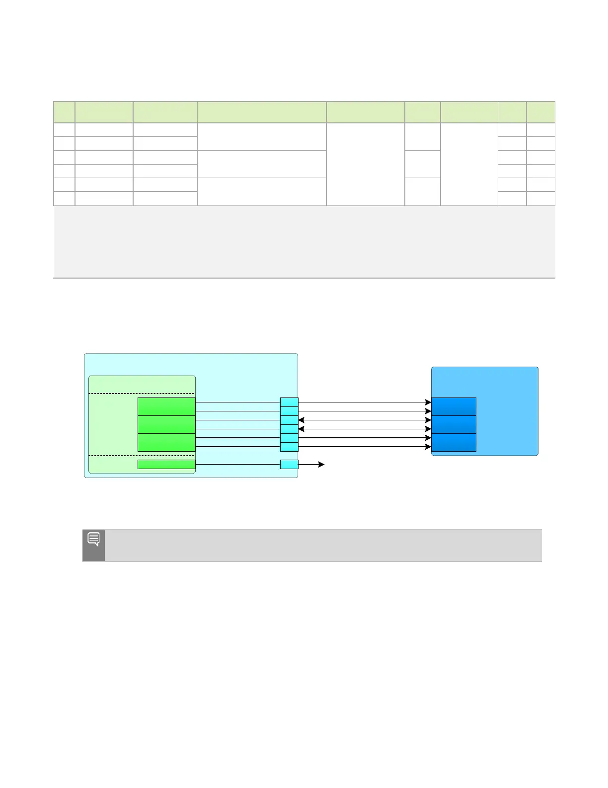
Figure 7-1. DSI 1 x 2 Lane Connection Example
Jetson
Tegra
DS I/CSI
DSI_A_CLK_P
DSI_A_CLK_N
Display
Connector (DSI)
D0P
D0N
D1P
D1N
CLKP
CLKN
DSI_A_D0_P
DSI_A_D0_N
DSI_A_D1_P
DSI_A_D1_N
SYS
LCD_BL_PWM
Optional Backlight PWM
78
76
72
70
84
82
DSI_CLK_P
DSI_CLK_N
DSI_D0_P
DSI_D0_N
DSI_D1_P
DSI_D1_N
GP IO 07
206
Note: If EMI/ESD devices are necessary, they must be tuned to minimize impact to signal quality,
which must meet the DSI spec. requirements for the frequencies supported by the design.

 Loading...


