PADS
NVIDIA Jetson Nano DG-09502-001_v2.1 | 68
Tegra is in slave mode. The FAN_TACH pin [GPIO8] is another input that could be affected by
noise on the signal edges. The SDMMC_CLK pin, while used to output the clock, also sample
the clock at the input to help with read timing. Therefore, the SDMMC_CLK pin may benefit
from enabling Schmitt-trigger mode. Care should be taken if the Schmitt-trigger mode setting
is changed from the default initialization mode as this can influence interface timing.
12.3 Pins Pulled and Driven High During
Power-ON
The Jetson Nano is powered up before the carrier board (See Section 5.1). Table 12-1 lists the
pins on Jetson Nano that default to being pulled or driven high. Care must be taken on the
carrier board design to ensure that any of these pins that connect to devices on the carrier
board (or devices connected to the carrier board) do not cause damage or excessive leakage to
those devices. Some of the ways to avoid issues with sensitive devices are:
External pull-downs on the carrier board that are strong enough to keep the signals low
are one solution, given that this does not affect the function of the pin.
Buffers or level shifters can be used to separate the signals from devices that may be
affected. The buffer and shifter should be disabled until the device power is enabled.
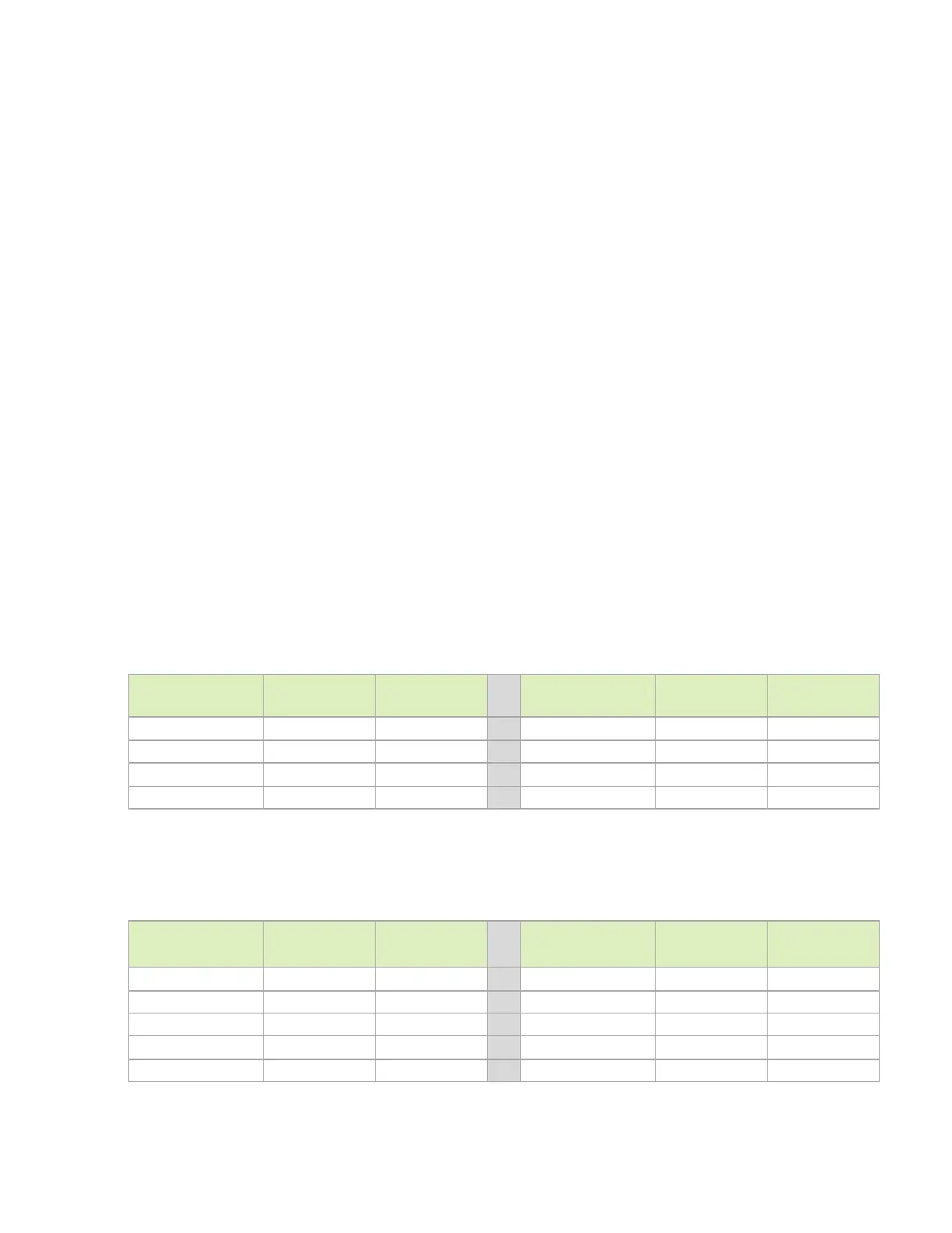
Table 12-1. Pins Pulled and Driven High by Tegra Prior to SYS_RESET*
Inactive
Jetson Nano Pin Power-ON
reset Default
Pull-up
Strength (kΩ)
Jetson Nano Pin Power-ON
reset Default
Pull-up
Strength (kΩ)
SYS_RESET* Driven high na SPI0_CS0* Internal pull-up ~15
SLEEP/WAKE* Internal pull-up ~100 SPI0_CS1* Internal pull-up ~15
FORCE_RECOVERY* Internal pull-up ~100 SPI1_CS0* Internal pull-up ~18
UART1_RXD Internal pull-up ~100 SPI1_CS1* Internal pull-up ~18
Table 12-2. Pins Pulled High on Module with External Resistors Prior
to SYS_RESET_IN* Inactive
Jetson Nano Pin Pull-up Supply
Voltage (V)
External
Pull-up (kΩ)
Jetson Nano Pin Pull-up Supply
Voltage (V)
External
Pull-up (kΩ)
I2C0_SCL/SDA 3.3 2.2 SPI1_CS0* 1.8 100
I2C1_SCL/SDA 3.3 2.2 SPI1_CS1* 1.8 100
I2C2_SCL/SDA 1.8 2.2 PCIE0_CLKREQ* 3.3 47
CAM_I2C_SCL/SDA 3.3 2.2 PCIE0_RST* 3.3 4.7
PCIE_WAKE* 3.3 100

 Loading...


