Miscellaneous Interfaces
NVIDIA Jetson Nano DG-09502-001_v2.1 | 59
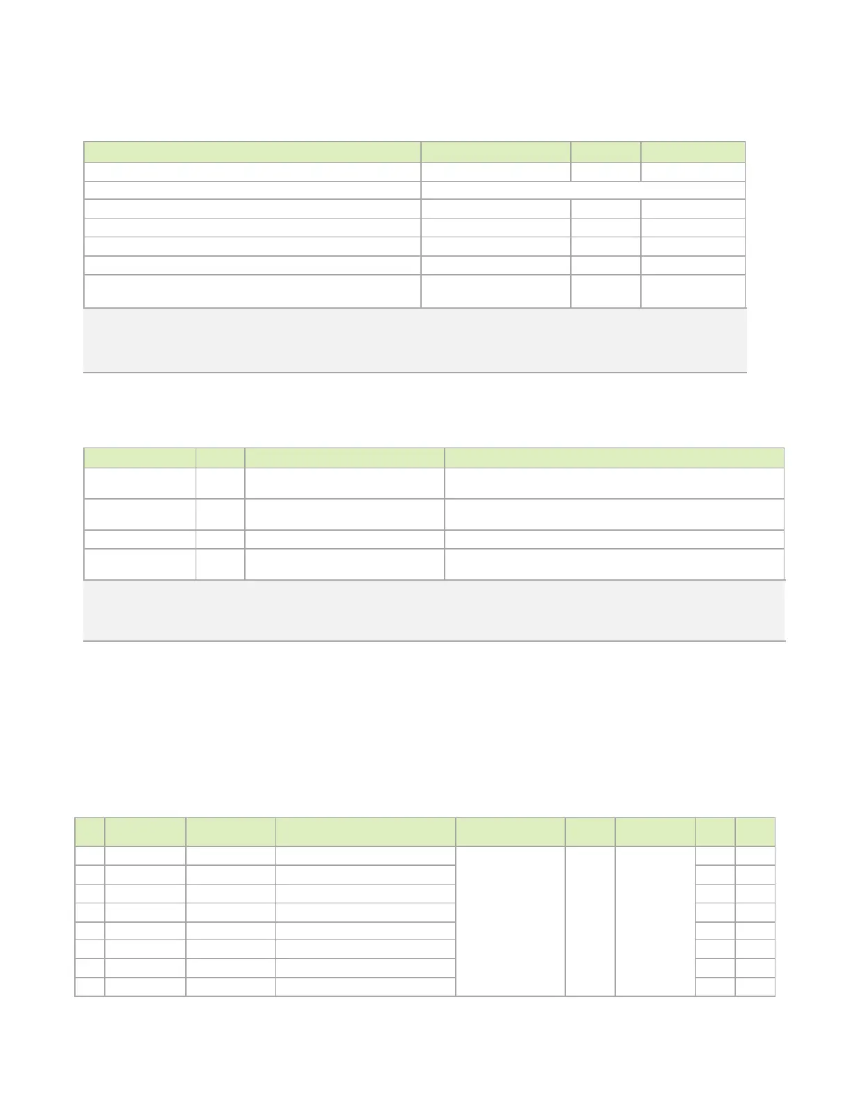
Table 11-2. I2C Interface Signal Routing Requirements
Parameter Requirement Units Notes
Max frequency Standard-mode / Fm / Fm+ 100 / 400 / 1000 kHz See Note 1
Topology Single ended, bi-directional, multiple masters/slaves
Max loading Standard-mode / Fm / Fm+ 400 pF Total of all loads
Reference plane
or
Trace impedance 50 – 60 Ω ±15%
Trace spacing 1x dielectric
Max trace length/delay Standard Mode
Fm, Fm+ Modes
3400 (~20)
1700 (~10)
ps (in)
Notes:
1. Fm = Fast-mode, Fm+ = Fast-mode Pl us.
2. Avoid routing I2C signals near noisy traces, supplies or components such as a switching power regulator.
3. No requirement for decoupling caps for PWR reference.
Table 11-3. I2C Signal Connections
Module Pin Name Type Termination Description
I/OD 2.2kΩ pull-ups to
on Jetson
Nano
I2C #0 Clock and Data. Connect to CLK and Data pins of any 3.3V devices
I/OD 2.2kΩ pull-ups to
on Jetson
Nano
I2C #1 Clock and Data. Connect to CLK and Data pins of 3.3V devices.
I/OD 2.2kΩ pull-ups to
on Jetson Nano
I2C #2 Clock and Data. Connect to CLK and Data pins of any 1.8V devices
I/OD
2.2kΩ pull-ups to
on Jetson
Nano
Camera I2C Clock and Data. Connect to CLK and Data pins of any 3.3V
devices
Notes:
1. If some devices require a different voltage level than others connected to the same I2C bus, level shifters are required.
2. For I2C interfaces that are pulled up to 1.8V, disable the E_IO_HV option for these pads. For I2C interfaces that are pulled up to 3.3V, enable the E_IO_HV
option. The E_IO_HV option is selected in the Pinmux registers.
11.2 SPI
The Jetson Nano brings out two of the Tegra SPI interfaces. See Figure 11-2.
Table 11-4. Jetson Nano SPI Pin Description
Pin # Module Pin Name Tegra X1 Signal Usage/Description
Usage on NVIDIA DevKit
Carrier Board
Direction Pin Type
Code
Power-on
Reset
89 SPI0_MOSI SPI1_MOSI SPI 0 Master Out / Slave In
Ex pansion header Bidir CMOS – 1.8V
LV_CZ pd
91 SPI0_SCK SPI1_SCK SPI 0 Clock LV_CZ pd
93 SPI0_MISO SPI1_MISO SPI 0 Master In / Slave Out LV_CZ pd
95 SPI0_CS0* SPI1_CS0 SPI 0 Chip Select 0 LV_CZ pu
97 SPI0_CS1* SPI1_CS1 SPI 0 Chip Select 1 LV_CZ pu
104 SPI1_MOSI SPI2_MOSI SPI 1 Master Out / Slave In CZ pd
106 SPI1_SCK SPI2_SCK SPI 1 Clock CZ pd
108 SPI1_MISO SPI2_MISO SPI 1 Master In / Slave Out CZ pd

 Loading...


