Display
NVIDIA Jetson Nano DG-09502-001_v2.1 | 36
7.3 HDMI and DP
A standard DP 1.2a or HDMI V2.0 interface is supported. These share the same set of interface
pins, so either DisplayPort or HDMI can be supported natively.
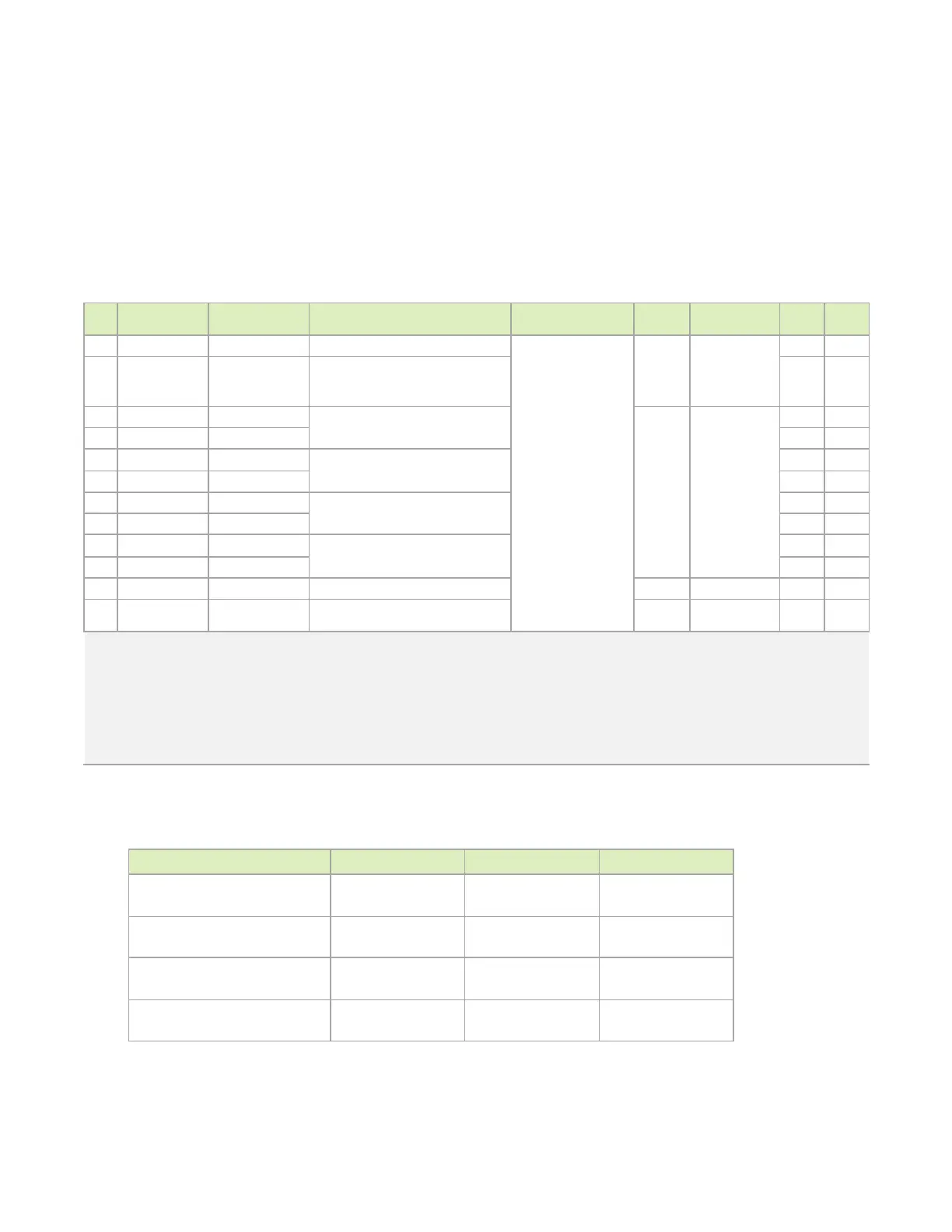
Table 7-8. Jetson Nano HDMI and DP Pin Description
Pin # Module Pin Name Tegra X1 Signal Usage/Description
Usage on NVIDIA DevKit
Carrier Board
Direction Pin Type
Code
Power-on
Reset
98 DP1_AUX_N DP_AUX_CH1_N DisplayPort 1 Aux– or HDMI DDC SDA
HDMI Conn.
Bidir
AC-Coupled on
Carrier Board
(eDP/DP) or Open-
Drain, 1.8V (3.3V
tolerant - DDC)
DP_AUX z
100 DP1_AUX_P DP_AUX_CH1_P DisplayPort 1 Aux+ or HDMI DDC SCL
DP_AUX z
63 DP1_TXD0_N HDMI_DP_TXDN0
DisplayPort 1 Lane 0 or HDMI Lane 2
Output
AC-Coupled on
carrier board
− z
65 DP1_TXD0_P HDMI_DP_TXDP0 − z
69 DP1_TXD1_N HDMI_DP_TXDN1
DisplayPort or HDMI Lane 1
−
z
71 DP1_TXD1_P HDMI_DP_TXDP1
−
z
75 DP1_TXD2_N HDMI_DP_TXDN2
DisplayPort 1 Lane 2 or HDMI Lane 0
− z
77 DP1_TXD2_P HDMI_DP_TXDP2 − z
81 DP1_TXD3_N HDMI_DP_TXDN3
DisplayPort 1 Lane 3– or HDMI Clk Lane
−
z
83 DP1_TXD3_P HDMI_DP_TXDP3 − z
96 DP1_HPD HDMI_INT_DP_HPD HDMI or Display Port Hot Plug Detect Input CMOS – 1.8V DD pd
94 HDMI_CEC HDMI_CEC HDMI CEC Bidir
Open Drain, 1.8V
(3.3V tolerant) DD z
Notes:
1. In the Type/Dir column, Output is from Jetson Nano. Input is to Jetson Nano. Bidir is for Bidirectional signals.
2. The directions for DP1_HPD and HDMI_CEC are true when used for these functions. Otherwise as GPIOs, the direction is bidirectional
3. The MPIO Pad Codes are described in the
Tegra X1 SoC Technical Reference Manual
“Multi-Purpose I/O Pins and Pin Multiplexing
(PinMux)” section for details.
4. The Power-on Reset State column indicates the pin state when reset is active and when it is deactivated before any changes are made by
software. “z” is tristate, pu/pd indicates internal weak pull-up/down resistor is enabled, 1/0 indicates actively driven high/low.
Table 7-9. DP and HDMI Pin Mapping
Module Pin Name Module Pin #s HDMI DP
DP1_TXD3_P
DP1_TXD3_N
TX3+
TX3–
DP1_TXD2_P
DP1_TXD2_N
TX2+
TX2–
DP1_TXD1_P
DP1_TXD1_N
TX1+
TX1–
DP1_TXD0_P
DP1_TXD0_N
TX0+
TX0–

 Loading...


