NVIDIA Jetson Nano DG-09502-001_v2.1 | 15
Chapter 6. USB and PCI Express
Jetson Nano allows multiple USB 2.0, USB 3.0 and PCIe interfaces to be brought out of the
module.
Note: In Table 6-1 and Table 6-2 the Type/Dir column, the Output is from Jetson Nano and the
Input is to Jetson Nano. Bidir is for bidirectional signals.
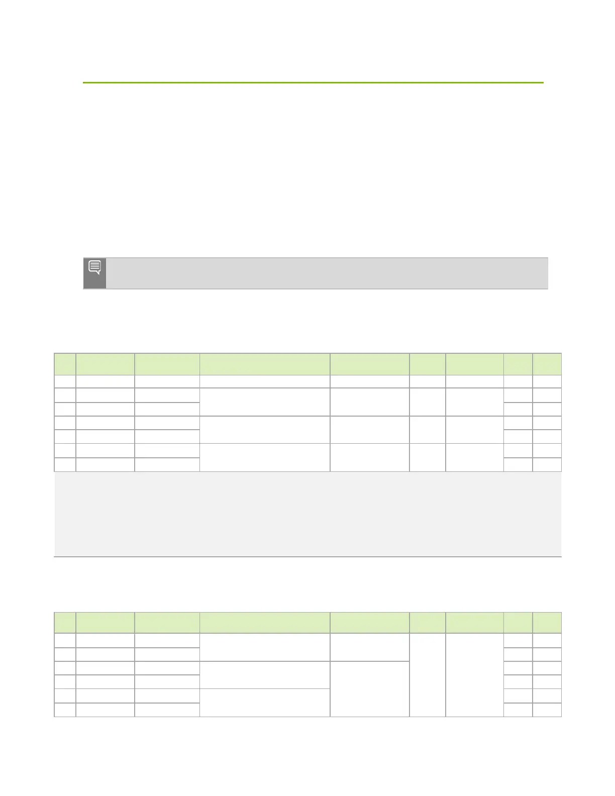
Table 6-1. Jetson Nano USB 2.0 Pin Descriptions
Pin # Module Pin Name Tegra X1 Signal Usage/Description
Usage on NVIDIA DevKit
Carrier Board
Direction Pin Type
Code
Power-on
Reset
87 GPIO00 US B_VBUS_EN0 GPIO #0 (USB 0 VBUS Detect) USB 2.0 Micro B Input Open Drain, 1.8V DD 0
109 USB0_D_N US B0_DN
USB 2.0 Port 0 Data USB 2.0 Micro B Bidir USB PHY
− 0
111 USB0_D_P US B0_DP − 0
115 USB1_D_N US B1_DN
USB 2.0 Port 1 Data US B Hub Bidir USB PHY
− 0
117 USB1_D_P US B1_DP − 0
121
USB2_D_N
US B2_DN
USB 2.0, Port 2 Data M.2 Key E Bidir USB PHY
−
0
123 USB2_D_P US B2_DP − 0
Notes:
1. In the Type/Dir column, Output is from Jetson Nano. Input is to Jetson Nano. Bidir is for Bidirectional signals.
2. The direction of GPIO00 is true when used for this function. Otherwise as a GPIO, the direction is bidirectional.
3. The MPIO Pad Codes are described in the
Tegra X1 SoC Technical Reference Manual
“Multi-Purpose I/O Pins and Pin Multiplexing
(PinMux)” section for details.
4. The Power-on Reset State column indicates the pin state when reset is active and when it is deactivated before any changes are made by
software. “z” is tristate, pu/pd indicates internal weak pull-up/down resistor is enabled, 1/0 indicates actively driven high/low.
Table 6-2. Jetson Nano USB 3.0 and PCIe Pin Descriptions
Pin # Module Pin Name Tegra X1 Signal Usage/Description
Usage on NVIDIA DevKit
Carrier Board
Direction Pin Type
Code
Power-on
Reset
131 PCIE0_RX0_N PEX_RX4N
PCIe #0 Receive 0 (PCIe Ctrl #0 Lane 0) M.2 Key E
Input
PCIe PHY, AC-
Coupled on carrier
board only if direct
connect t o dev ice
− −
133 PCIE0_RX0_P PEX_RX4P
− −
137 PCIE0_RX1_N PEX_RX3N
PCIe #0 Receive 1 (PCIe Ctrl #0 Lane 1)
Not Assigned
− −
139 PCIE0_RX1_P PEX_RX3P − −
149 PCIE0_RX2_N PEX_RX2N
PCIe #0 Receive 2 (PCIe Ctrl #0 Lane 2)
− −
151 PCIE0_RX2_P PEX_RX2P
− −

 Loading...


