Power
NVIDIA Jetson Nano DG-09502-001_v2.1 | 12
Pin # Module Pin Nam e Tegra X1 Signal Usage/Description
Usage on NVIDIA DevKit
Carrier Board
Direction Pin Type
is controlled by system software and should
not be modified.
Notes:
1. In the Type/Dir column, Output is from Jetson Nano. Input is to Jetson Nano. Bidir is for Bidirectional signals.
2. The directions for FORCE_RECOVERY* and SLEEP/WAKE* signals are true when used for those functions. Otherwise as GPIOs, the
direction is bidirectional.
3. The MPIO Pad Codes are described in the
Tegra X1 SoC Technical Reference Manual
“Multi-Purpose I/O Pins and Pin Multiplexing
(PinMux)” section for details.
4. The Power-on Reset State column indicates the pin state when reset is active and when it is deactivated before any changes are made by
software. “z” is tristate, pu/pd indicates internal weak pull-up/down resistor is enabled, 1/0 indicates actively driven high/low.
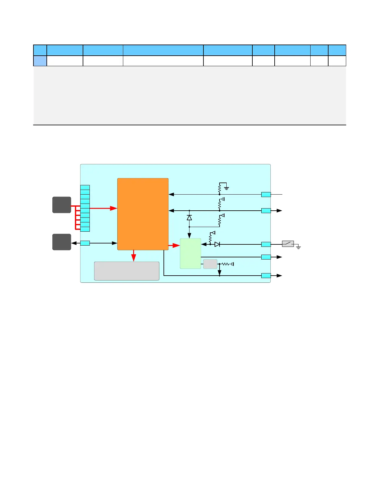
Figure 5-1. Jetson Nano Power and Control Block Diagram
Jetson Nano
Main 5V
Power
Source
255
256
257
258
259
260
235
Memory/Peripherals
LPDDR4, eMMC,
Ethernet
Power Subsystem
Tegra X1
PMIC_BBAT
VDD_IN
233
240
239
237
POWE R_EN
SYS_RESET*
SLEEP /WAKE*
MOD_SLEEP *
SHUTDOWN_REQ*
To Carrier Board – Used to force
power off if shutdown request
(T he rmal S hut down, Powe r Bad o r
Software Shutdown, etc.) is received
From Carrier Board power
ON/ OFF c ont rol lo gic
System Reset from Carrier
Board. Carrier Board power
enable f rom Module.
Optional Sleep/Wake Button
SLE EP/W AKE
Super
Cap or
Li Cell
251
252
253
254
178
Indicates Module is entering
Sleep (LP0) mode
10 0k Ω4. 7kΩ
VDD_1V8
4. 7kΩ
VDD_1V8
10 0k Ω
VDD_1V8
Lev el
Shifter
10 0k Ω
VDD_IN (5V)
5.1 Power Supply and Sequencing
The carrier board receives the main power source and uses this to generate the enable to
Jetson Nano (
POWER_EN) after the carrier board has ensured the main supply is stable and the
associated decoupling capacitors have charged. The carrier board supplies are not enabled at
this time. Once POWER_EN is driven active (high), Jetson Nano begins to Power-ON. When the
module Power-ON sequence has completed, the
SYS_RESET* signal is driven inactive (high) and
this is used by the carrier board to enable its various supplies.
SYS_RESET* is bidirectional and
can be driven by the carrier board to reset Jetson Nano, which results in a full system power
cycle. The SHUTDOWN_REQ* signal from Jetson Nano can be driven active (low) if the system
must be shut down, due to a critical thermal issue, etc. The power control logic on the carrier
board should drive POWER_EN inactive (low) if SHUTDOWN_REQ* is asserted. The SHUTDOWN_REQ*
signal is latched to a logic low level when the
VDD_IN supply is at or below 4.2V.

 Loading...


