SD Card and SDIO
NVIDIA Jetson Nano DG-09502-001_v2.1 | 52
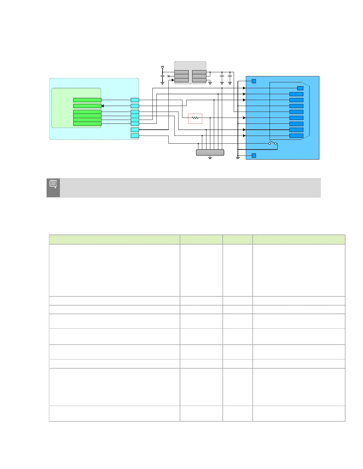
Figure 9-1. SD Card Connection Example
ESD
DATA2
DATA3
CMD
VDD
CLK
GND
DATA0
DATA1
C_DETECT
COMMON
VDD_3V3_ SYS
TPS22917DBVT
Load S witch
VO UTVIN
CT
SDMMC_V DD_E N
GND
0Ω
Jetson
Tegra
SDMMC3
SDMMC3_ CLK
SDMMC3_ CMD
SDMMC3_ DAT3
SDMMC_CLK
SDMMC_CMD
SDMMC_DAT0
SDMMC_DAT1
SDMMC_DAT2
SDMMC_DAT3
GP IO
GP IO
SDMMC3_ DAT2
SDMMC3_ DAT1
SDMMC3_ DAT0
227
229
#
#
219
221
223
225
0.1uF 10uF
EN
QOD
0.1uF
GND
SDMMC_CD
See Note
Note: Having 0Ω, 0402 resistor is recommended in case of issues with EMI where it can be
replaced with an appropriate device.
Table 9-2. SD Card and SDIO Interface Signal Routing Requirements
Parameter Requirement Units Notes
Max frequency 3.3V Signaling DS
HS
1.8V Signaling SDR12
SDR25
SDR50
SDR104
DDR50
25 (12.5)
50 (25)
25 (12.5)
50 (25)
100 (50)
208 (104)
50 (50)
MHz
(MB/s)
See Note 1
Topology Point to point
Reference plane
or
See Note 2
Trace impedance 50
Ω
±15%. 45Ω optional depending on stack-
up
Max via count PTH
HDI
4
10
Independent of stack-up layers.
Depends on stack-up layers.
Via proximity (Signal to reference)
< 3.8 (24) mm (ps) Up to four signal vias can share 1
return via
Trace spacing Microstrip / Stripline 4x / 3x dielectric
Trace length
SDR50 / SDR25 / SDR12 / HS / DS Min
Max
SDR104 / DDR50 Min
Max
16 (100)
139 (876)
16 (100)
83 (521)
mm (ps)
Max trace length/delay skew in/between
and
/
14 (87.5)
mm (ps)
See Note 3

 Loading...


