Display
NVIDIA Jetson Nano DG-09502-001_v2.1 | 44
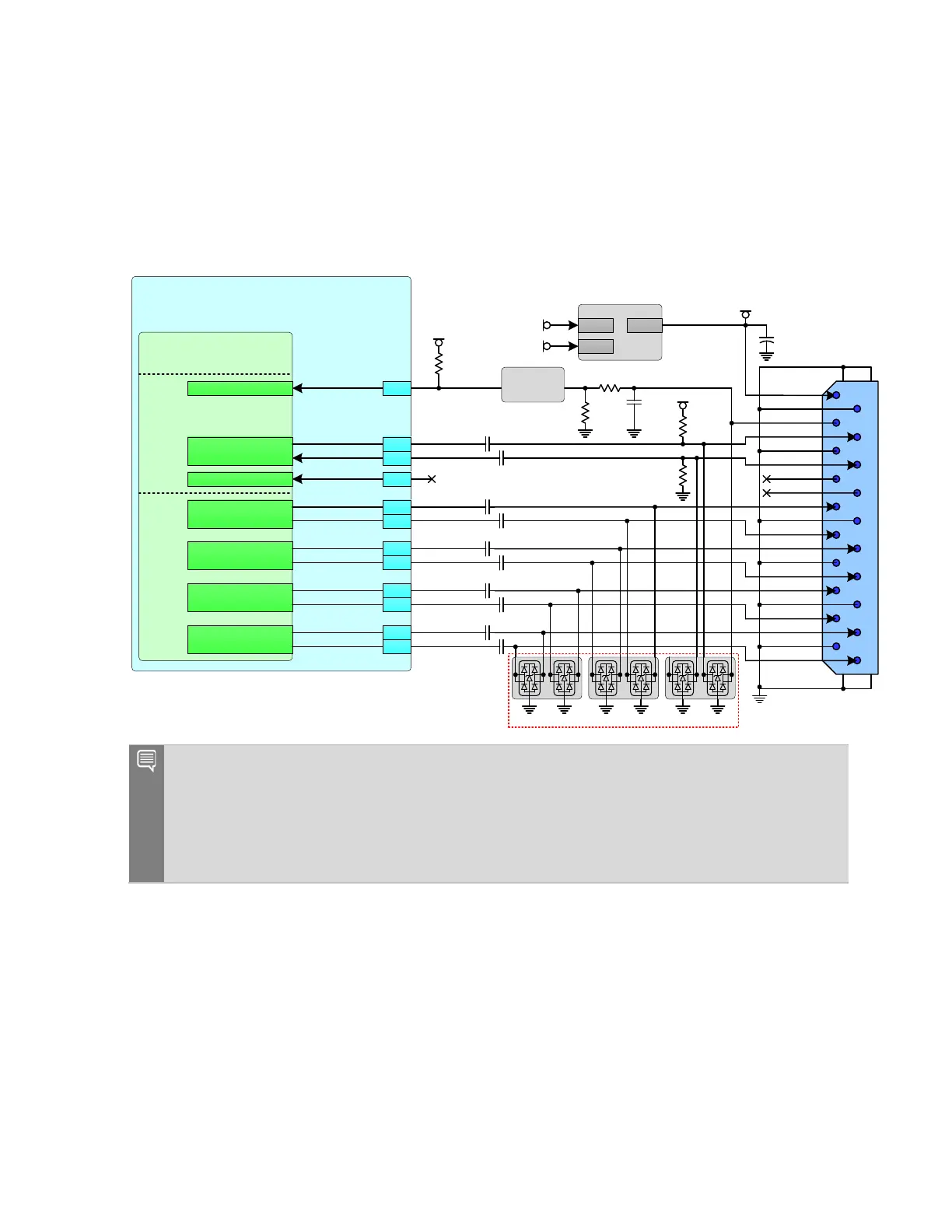
7.3.2 DP on DP1 Pins
Figure 7-21 shows the DisplayPort connection.
Figure 7-21. DP Connection Example
0. 1uF
0. 1uF
0. 1uF
0. 1uF
0. 1uF
0. 1uF
0. 1uF
0. 1uF
0. 1uF
0. 1uF
10 0k Ω
VDD_3V3 _SYS
10 0k Ω
VDD_3V3 _EDP
DP
Conn
.
PWR
PWR_RET
HPD
AUXN
GND
AUXP
CEC_DP
MODE
LA NE _3 N
GND
LA NE _3 P
LA NE _2 N
GND
LA NE _2 P
LA NE _1 N
GND
LA NE _1 P
LA NE _0 N
GND
LA NE _0 P
1
3
5
11
7
9
13
15
17
19
2
10
12
6
8
14
16
18
4
20
T PD4E 05U06
Jetson
Tegra
- HDMI
HDMI_DP_TXDP3
HDMI_DP_TXDN3
HDMI_DP_TXDP2
HDMI_DP_TXDN2
HDMI_DP_TXDP1
HDMI_DP_TXDN1
HDMI_DP_TXDP0
HDMI_DP_TXDN0
DP_AUX_CH1_N
DP_AUX_CH1_P
HDMI_INT_DP_HPD
DP
HDMI
HDMI_CEC
DP1_HPD
DP1_AUX_N
DP1_AUX_P
HDMI_CEC
DP1_TXD3_N
DP1_TXD3_P
DP1_TXD2_N
DP1_TXD2_P
DP1_TXD1_N
DP1_TXD1_P
DP1_TXD0_N
DP1_TXD0_P
96
100
98
94
65
63
71
69
77
83
81
75
0. 1uF
VDD_3V3 _SYS
3V 3_IO_ PG
VDD_1V8
10 kΩ
10 kΩ
10 kΩ
Load Switch
EN
IN
OUT
Lev el Shifte r
1.8V 3.3V
Notes:
1. Level shifter required on DP1_HPD to avoid the pin from being driven when Jetson Nano is
off. The level shifter must be non-inverting (preserve the polarity of the HPD signal from the
display).
2. Any EMI/ESD included on the HDMI_DP pins must be suitable for the highest frequency
modes supported (<1pf capacitive load recommended).

 Loading...


