Miscellaneous Interfaces
NVIDIA Jetson Nano DG-09502-001_v2.1 | 60
Pin # Module Pin Name Tegra X1 Signal Usage/Description
Usage on NVIDIA DevKit
Carrier Board
Direction Pin Type
Code
Power-on
Reset
110 SPI1_CS0* SPI2_CS0 SPI 1 Chip Select 0 CZ pu
112 SPI1_CS1* SPI2_CS1 SPI 1 Chip Select 1 CZ pu
Notes:
1. In the Type/Dir column, Output is from Jetson Nano. Input is to Jetson Nano. Bidir is for Bidirectional signals.
2. The directions for SPI[1:0]x are true when used for those functions. Otherwise as GPIOs, the directions are bidirectional.
3. The MPIO Pad Codes are described in the
Tegra X1 SoC Technical Reference Manual
“Multi-Purpose I/O Pins and Pin Multiplexing
(PinMux)” section for details.
4. The Power-on Reset State column indicates the pin state when reset is active and when it is deactivated before any changes are made by
software. “z” is tristate, pu/pd indicates internal weak pull-up/down resistor is enabled, 1/0 indicates actively driven high/low.
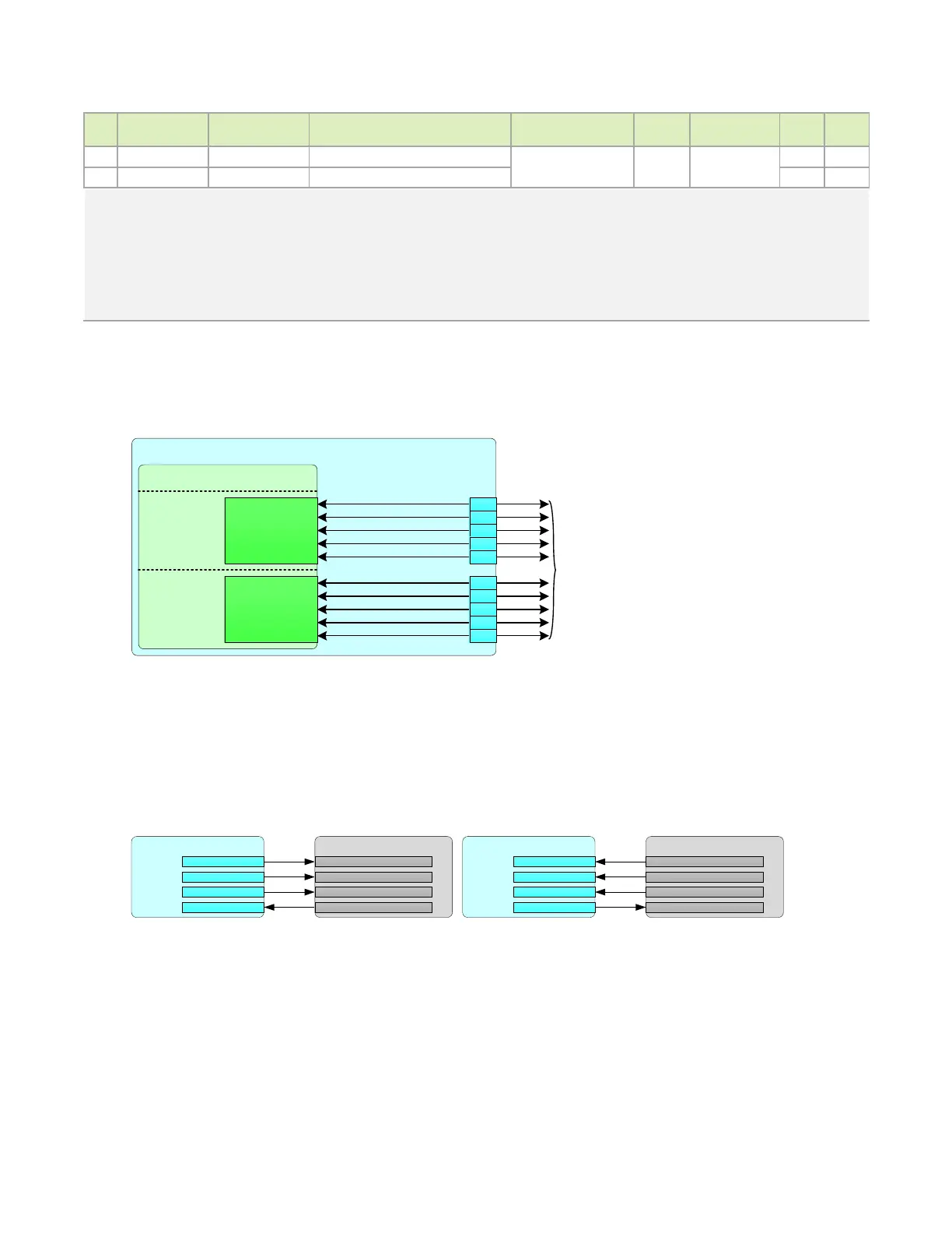
Figure 11-2. SPI Connections
Jetson
Tegra – SPI
SPI
SPI0_SCK
SP I 0_ M I SO
SP I 0_ M OSI
SP I 0_ CS0 *
SP I 0_ CS1 *
SPI1_SCK
SP I _M I SO
SP I 1_ M OSI
SP I 1_ CS0 *
SP I 1_ CS1 *
SPI1_SCK
SPI1_MISO
SPI1_MOSI
SPI1_CS0
SPI1_CS1
Routed to 40-pin
Expansion Header on
DevKit carrier board
91
89
93
95
97
SPI2_SCK
SPI2_MISO
SPI2_MOSI
SPI2_CS0
SPI2_CS1
106
104
108
110
112
AUDIO_HV
Figure 11-3 shows the basic connections used.
Figure 11-3. Basic SPI Master and Slave Connections
Jetson Master
SPIn_CSx
SP I n_ SCK
SP I n_ MOSI
SP I n_
MISO
SPI Slave Device
CS (Chip Select)
CLK ( Clock)
MOSI (Ma ster out, Slave in)
MISO (Ma ster in, Slave out)
Jetson Slave
SPIn_CSx
SP I n_ SCK
SP I n_ MOSI
SP I n_ MISO
SPI Master Device
CS (Chip Select)
CLK ( Clock)
MOSI (Ma ster out, Slave in)
MISO (Ma ster in, Slave out)

 Loading...


