NVIDIA Jetson Nano DG-09502-001_v2.1 | 54
Chapter 10. Audio
Tegra supports multiple PCM/I2S audio interfaces and includes a flexible audio-port switching
architecture.
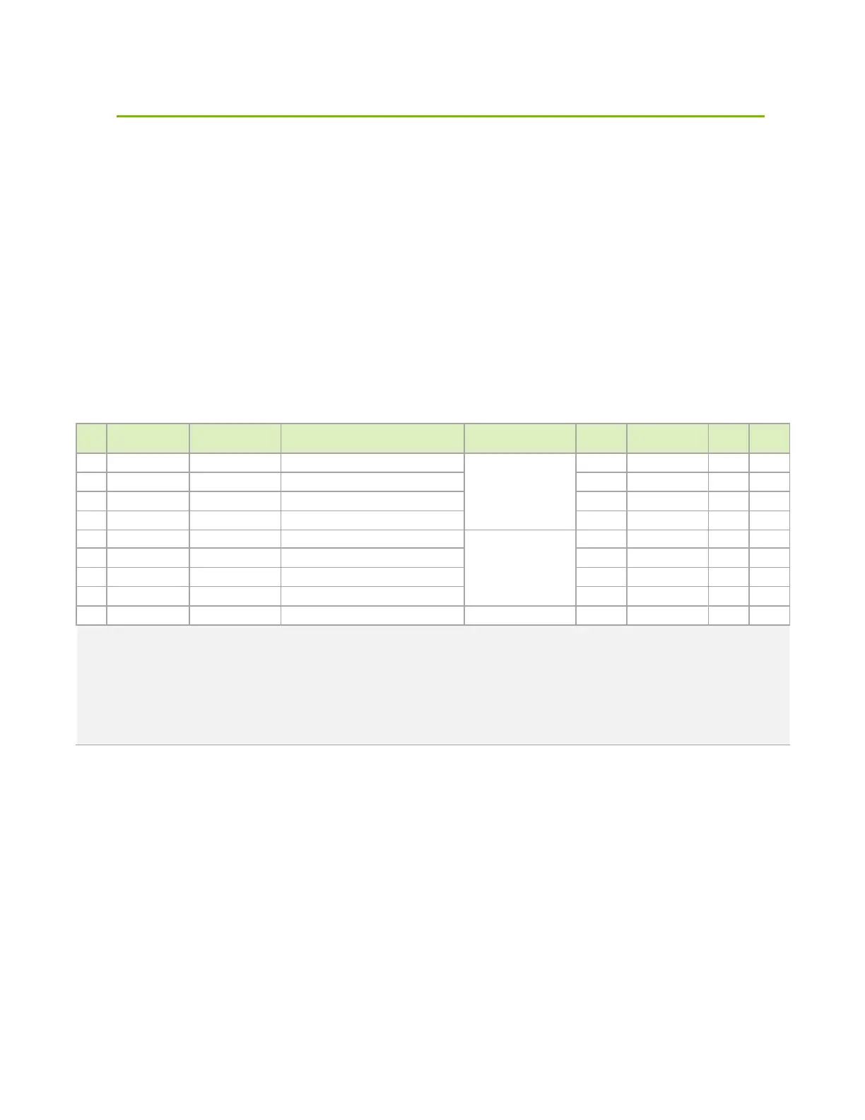
Table 10-1. Jetson Nano Audio Pin Description
Pin # Module Pin Name Tegra X1 Signal Usage/Description
Usage on NVIDIA DevKit
Carrier Board
Direction Pin Type
Code
Power-on
Reset
193 I2S0_DOUT DAP4_DOUT I2S Audio Port 0 Data Out
Ex pansion Header
Output CMOS – 1.8V ST pd
195 I2S0_DIN DAP4_DIN I2S Audio Port 0 Data In Input CMOS – 1.8V ST pd
197 I2S0_FS DAP4_FS I2S Audio Port 0 Left/Right Clock Bidir CMOS – 1.8V ST pd
199 I2S0_SCLK DA P4_SCLK I2S Audio Port 0 Clock Bidir CMOS – 1.8V ST pd
220 I2S1_DOUT DMIC2_CLK I2S Audio Port 1 Data Out
M.2 Key E
Bidir CMOS – 1.8V ST pd
222 I2S1_DIN DMIC1_DAT I2S Audio Port 1 Data In Input CMOS – 1.8V ST pd
224 I2S1_FS DMIC1_CLK I2S Audio Port 1 Left/Right Clock Bidir CMOS – 1.8V ST pd
226 I2S1_SCLK DMIC2_DAT I2S Audio Port 1 Clock Bidir CMOS – 1.8V ST pd
211 GPIO09 AUD_MCLK GPIO #9 or Audio Codec Master Clock Ex pansion Header Output CMOS – 1.8V ST pd
Notes:
1. In the Type/Dir column, Output is from Jetson Nano. Input is to Jetson Nano. Bidir is for Bidirectional signals.
2. The directions for I2S[1:0]x and GPIO09 are true when used for those functions. Otherwise as GPIOs, the directions are bidirectional.
3. The MPIO Pad Codes are described in the
Tegra X1 SoC Technical Reference Manual
“Multi-Purpose I/O Pins and Pin Multiplexing
(PinMux)” section for details.
4. The Power-on Reset State column indicates the pin state when reset is active and when it is deactivated before any changes are made by
software. “z” is tristate, pu/pd indicates internal weak pull-up/down resistor is enabled, 1/0 indicates actively driven high/low.

 Loading...


