NVIDIA Jetson Nano DG-09502-001_v2.1 | 11
Chapter 5. Power
Power for the module is supplied on the VDD_IN pins and is nominally 5.0V (see the
Jetson
Nano Data Sheet
for supply tolerance and maximum current).
CAUTION: Jetson Nano is not hot-pluggable. When installing the module, the main power supply
should not be connected. Before removing the module, the main power supply (to VDD_IN pins)
must be disconnected and allowed to discharge below 0.6V.
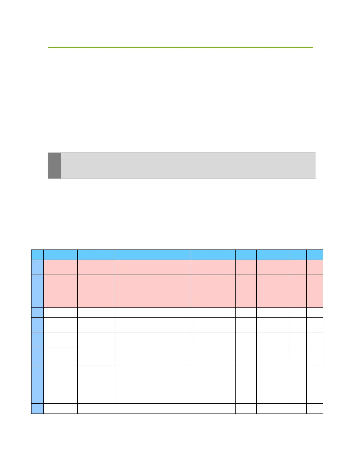
Table 5-1. Jetson Nano Power and System Pin Descriptions
Pin # Module Pin Nam e Tegra X1 Signal Usage/Description
Usage on NVIDIA DevKit
Carrier Board
Direction Pin Type
↓
Main power – Supplies PMIC and other
regulators
235 PMIC_BBA T −
PMIC Battery Back-up. Optionally used to
provide back-up power for the Real-Time-
Clock (RTC). Connects to Lithium Cell or super
capacitor on Carrier Board. PMIC is source
when charging cap or coin cell. Super cap or
coin cell is source when system is
Batt ery Back-up using
Super-capacitor
Bidir 1.65V-5.5V
214
BUTTON_VOL_UP Force Recovery strap pin Automation header Input CMOS – 1.8V ST pu
240 SLEEP/WAKE* BUTTON_PWR_ON
Sleep/Wake. Configured as GPIO for optional
use to indicate the system should enter or exit
Automation header Input CMOS – 5.0V ST pu
233 SHUTDOWN_REQ* −
Used by the module to request the carrier
board to shut down. 100kΩ pull-up to VDD_IN
System Output Open Drain, 5.0V
237 POWER_EN
(PMIC EN0 through
convert er logic)
Signal for module on/off: high level on, low
lev el off. Connects to module PMIC EN0
through converter logic. 100kΩ pulldown on
System Input Analog 5.0V
239 SYS_RESET* SYS_RESET_IN_N
Module Reset. Reset to the module when
driven low by the carrier board. Used as
carrier board supply enable when driven high
by the module. when module power
sequence is complete. Used to ensure proper
power on/off sequencing for between module
and carrier board supplies. 4.7kΩ pull-up to
Automation header Bidir Open Drain, 1.8V JT_RST 1
178 MOD_SLEEP* GPIO_PA6
Indicates the module sleep status. Low is in
sleep mode, high is normal operation. This pin
HDMI termination pull-
down FET control disable
Output CMOS – 1.8V ST z

 Loading...


