EasyManuals Logo

Nvidia JETSON NANO Product Design Guide

Nvidia JETSON NANO
84 pages
To Next Page IconTo Next Page
To Previous Page IconTo Previous Page
Page #28 background imageLoading...
Page #28 background image
USB and PCI Express
NVIDIA Jetson Nano DG-09502-001_v2.1 | 20
Parameter Requirement Units Notes
General: See Chapter 15 for guidelines related to serpentine routing, routing over voids and noise coupling
Note:
1. Longer trace lengths may be possible if the total trace loss is equal to or better than the target. If the loss is greater, the max trace lengths will need to
be reduced.
2. Recommend trace length matching to <1ps before vias or any discontinuity to minimize common mode conversion.
3. Place GND vias as symmetrically as possible to data pair vias.
The following figures show the USB 3.0 interface signal routing requirements.
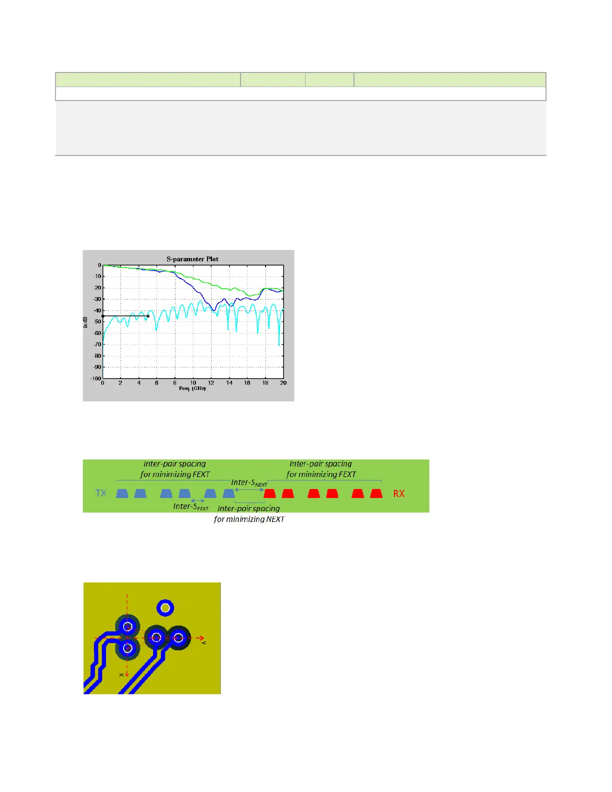
Figure 6-2. IL/NEXT Plot
Figure 6-3. Trace Spacing for TX/RX Non-Interleaving
Figure 6-4. Via Structures

Table of Contents

Other manuals for Nvidia JETSON NANO

Questions and Answers:

Question and Answer IconNeed help?

Do you have a question about the Nvidia JETSON NANO and is the answer not in the manual?

Nvidia JETSON NANO Specifications

General IconGeneral
GPU128-core NVIDIA Maxwell
Memory4 GB LPDDR4
Storage16 GB eMMC 5.1
Video Encode4K @ 30 | 4x 1080p @ 30 | 9x 720p @ 30 (H.264/H.265)
Dimensions100 mm x 80 mm x 29 mm
CPUQuad-core ARM Cortex-A57
Video Decode4K @ 60 | 2x 4K @ 30 | 8x 1080p @ 30 | 18x 720p @ 30 (H.264/H.265)
ConnectivityGigabit Ethernet
DisplayHDMI 2.0
USBUSB 3.0
OtherGPIO, I2C, SPI, UART
Operating SystemLinux
Power5V
Camera12x (MIPI CSI-2) DPHY lanes

Related product manuals