EasyManuals Logo

Nvidia JETSON NANO Product Design Guide

Nvidia JETSON NANO
84 pages
To Next Page IconTo Next Page
To Previous Page IconTo Previous Page
Page #61 background imageLoading...
Page #61 background image
SD Card and SDIO
NVIDIA Jetson Nano DG-09502-001_v2.1 | 53
Parameter Requirement Units Notes
SDR50 / SDR25 / SDR12 / HS / DS
SDR104 / DDR50
2 (12.5)
Keep CLK, CMD and DATA traces away from other signal traces or unrelated power traces/areas or power supply components
Notes:
1. Actual frequencies may be lower due to clock source/divider limitations.
2. If PWR, 0.01uF decoupling cap required for return current.
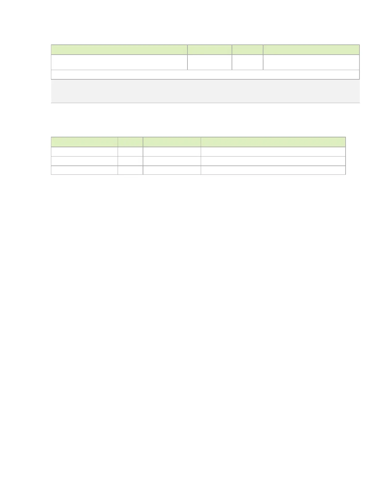
Table 9-3. SD Card and SDIO Signal Connections
Function Signal Name Type Termination Description
SDMMC_CLK O
SD Card / SDIO Clock: Connect to CLK pin of device.
SDMMC_CMD I/O SD Card / SDIO Command: Connect to CMD pin of device
SDMMC_D[3:0] I/O SD Card / SDIO Data: Connect to Data pins of device

Table of Contents

Other manuals for Nvidia JETSON NANO

Questions and Answers:

Question and Answer IconNeed help?

Do you have a question about the Nvidia JETSON NANO and is the answer not in the manual?

Nvidia JETSON NANO Specifications

General IconGeneral
GPU128-core NVIDIA Maxwell
Memory4 GB LPDDR4
Storage16 GB eMMC 5.1
Video Encode4K @ 30 | 4x 1080p @ 30 | 9x 720p @ 30 (H.264/H.265)
Dimensions100 mm x 80 mm x 29 mm
CPUQuad-core ARM Cortex-A57
Video Decode4K @ 60 | 2x 4K @ 30 | 8x 1080p @ 30 | 18x 720p @ 30 (H.264/H.265)
ConnectivityGigabit Ethernet
DisplayHDMI 2.0
USBUSB 3.0
OtherGPIO, I2C, SPI, UART
Operating SystemLinux
Power5V
Camera12x (MIPI CSI-2) DPHY lanes

Related product manuals