Display
NVIDIA Jetson Nano DG-09502-001_v2.1 | 30
7.1.1 MIPI DSI and CSI Design Guidelines
Table 7-3 details the MIPI DSI and CSI interface signal routing requirements.
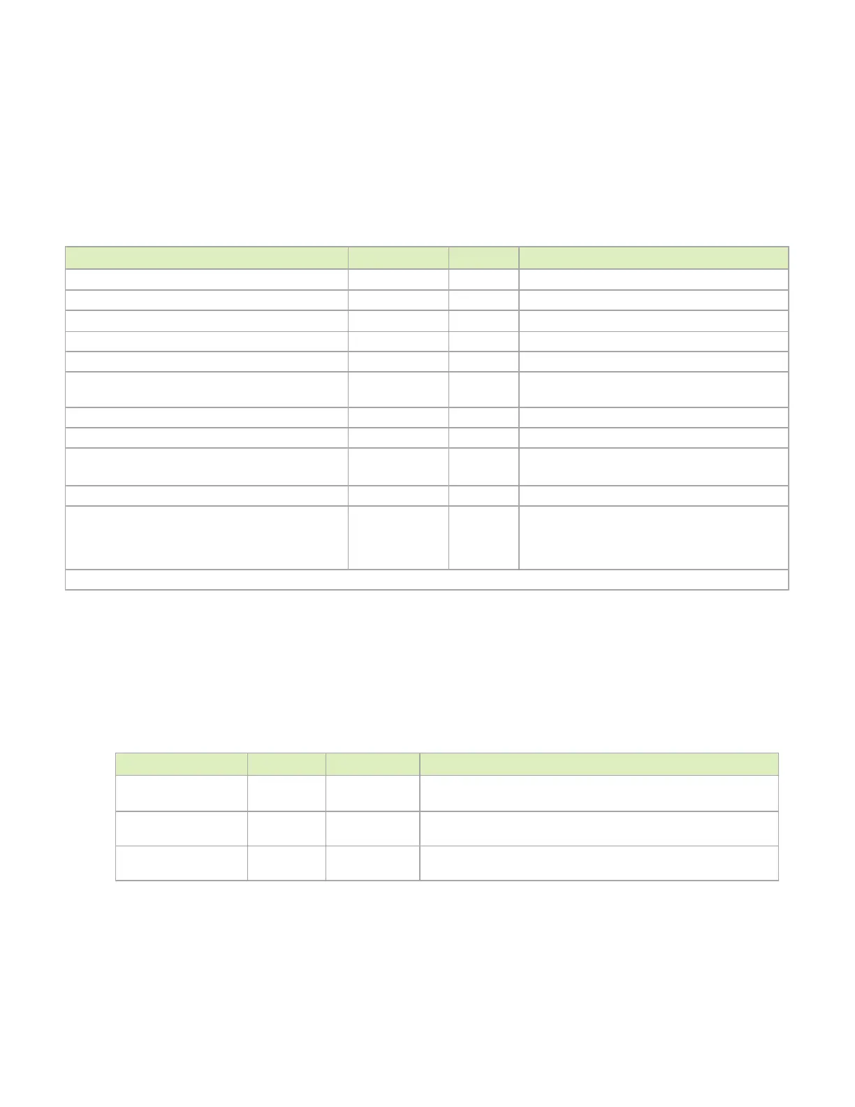
Table 7-3. MIPI DSI and CSI Interface Signal Routing Requirements
Parameter Requirement Units Notes
Max frequency/data rate (per data lane) 750 / 1500 MHz/Mbps
Number of loads 1 load
Reference plane GND
Trace impedance Diff pair / SE 90-100 / 45-50 Ω
±10%
Via proximity (signal to reference) < 0.65 (3.8) mm (ps)
Intra-pair trace spacing 0.15mm mm Can be adjusted to meet Differential Impedance.
Loosely Coupled Diff. Pair recommended by Spec.
Inter-pair trace spacing Microstrip / Stripline 4x / 3x dielectric
Max PCB breakout length 5 mm
Max trace delay 1 Gbps
1.5 Gbps
1100
800
ps
Max intra-pair skew 1 ps
Max trace delay skew between
and
5 ps
includes all the data lines associated with a
single clock. This may be 2 differential data lanes
for a x2 interface, or 4 differential data lanes for a
x4 interface.
Keep critical traces away from other signal traces or unrelated power traces/areas or power supply components
7.1.2 MIPI DSI and CSI Connection Guidelines
Table 7-4 details the MIPI DSI signal connections.
Table 7-4. MIPI DSI Signal Connections
Module Pin Name Type Termination Description
DSI_CLK_N/P DIFF OUT DSI Differential Clock: Connect to CLKn and CLKp pins of the primary
DSI display
DSI_D[1:0]_N/P DIFF OUT DSI Differential Data Lanes 1:0: Connect to corresponding data lanes
of DSI display.
GPIO07 O Optional LCD Backlight Pulse Width Modulation: Connect to LCD
backlight solution PWM input if supported

 Loading...


