NVIDIA Jetson Nano DG-09502-001_v2.1 | 51
Chapter 9. SD Card and SDIO
Jetson Nano uses one SDMMC interface for on-module eMMC (SDMMC4 on Tegra) and brings
one to the connector pins for SD Card or SDIO use.
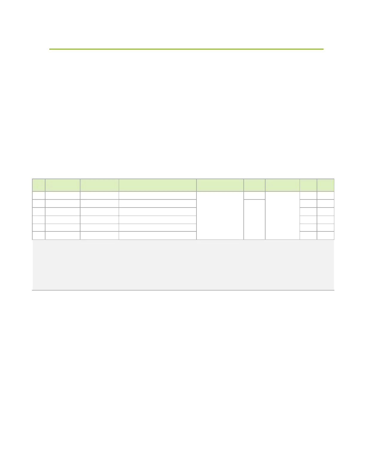
Table 9-1. Jetson Nano SDIO Pin Description
Pin # Module Pin Name Tegra X1 Signal Usage/Description
Usage on NVIDIA DevKit
Carrier Board
Direction Pin Type
Code
Power-on
Reset
229 SDMMC_CLK SDMMC3_CLK SD Card or SDIO Clock
Not Assigned
Output
CMOS – 1.8V/3.3V
CZ pd
227 SDMMC_CMD SDMMC3_CMD SD Card or SDIO Command
Bidir
CZ pu
219 SDMMC_DAT0 SDMMC3_DAT0 SD Card or SDIO Data 0 CZ pu
221 SDMMC_DAT1 SDMMC3_DAT1 SD Card or SDIO Data 1 CZ pu
223 SDMMC_DAT2 SDMMC3_DAT2 SD Card or SDIO Data 2 CZ pu
225 SDMMC_DAT3 SDMMC3_DAT3 SD Card or SDIO Data 3 CZ pu
Notes:
1. In the Type/Dir column, Output is from Jetson Nano. Input is to Jetson Nano. Bidir is for Bidirectional signals.
2. The directions for SDMMC_x and GPIO08 are true when used for these functions. Otherwise as GPIOs, the directions are bidirectional.
3. The MPIO Pad Codes are described in the
Tegra X1 SoC Technical Reference Manual
“Multi-Purpose I/O Pins and Pin Multiplexing
(PinMux)” section for details.
4. The Power-on Reset State column indicates the pin state when reset is active and when it is deactivated before any changes are made by
software. “z” is tristate, pu/pd indicates internal weak pull-up/down resistor is enabled, 1/0 indicates actively driven high/low.

 Loading...


