RL78/F13, F14 CHAPTER 21 INTERRUPT FUNCTIONS
R01UH0368EJ0210 Rev.2.10 1480
Dec 10, 2015
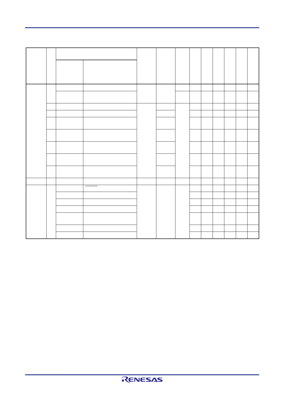
Table 21-1. Interrupt Source List (4/4)
Interrupt
Type
Default Priority
Note 1
Interrupt Source
Internal/
External
Vector
Table
Address
Basic Configuration
Type
Note 2
80, 100-pin
64-pin
48-pin
32-pin
30-pin
20-pin
Name Trigger
INTLIN1WUP
Note 6
LIN1 reception pin input (E)
Note 5
Note 5
Note 5
49 INTLIN1TRM LIN1 transmission Internal 0066H (A)
Note 5
Note 5
Note 5
50 INTLIN1RVC LIN1 reception end 0068H
Note 5
Note 5
Note 5
51 INTLIN1STA/
INTLIN1
LIN1 reception status/LIN1
interrupt
006AH
Note 5
Note 5
Note 5
52 INTTM14 End of TAU1 channel 4
count/capture
006CH
Note 5
Note 5
Note 5
53 INTTM15 End of TAU1 channel 5
count/capture
006EH
Note 5
Note 5
Note 5
54 INTTM16 End of TAU1 channel 6
count/capture
0070H
Note 5
Note 5
Note 5
55 INTTM17 End of TAU1 channel 7
count/capture
0072H
Note 5
Note 5
Note 5
Software BRK Execution of BRK instruction 007EH (F)
Reset RESET RESET pin input 0000H
POR Power-on-reset
LVD Voltage detection
Note 3
WDT Overflow of watchdog timer
TRAP Execution of illegal
instruction
Note 4
IAW Illegal-memory access
CLM Main clock oscillation stop
Notes 1. The default priority determines the sequence of interrupts if two or more maskable interrupts occur
simultaneously. Zero indicates the highest priority and 55 indicates the lowest priority.
2. Basic configuration types (A) to (F) correspond to (A) to (F) in Figure 21-1.
3. When bit 7 (LVIMD) of the voltage detection level register (LVIS) is set to 1.
4. When the instruction code in FFH is executed.
Reset by the illegal instruction execution not issued by emulation with the in-circuit emulator or on-chip debug
emulator.
5. Provided only in Group E products.
6. Select INTP12 and INTLIN1WUP by the ISC3 bit in the ISC register.
 Loading...


