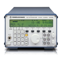
V L F > H F R E C E I V E R S
f
R & S E K 8 9 5 / R & S E K 8 9 6
User Manual
f
Processor
1.3.5 Processor
1.3.5.1 Design
The processor consists of a printed circuit
board, a set of screens, two screw tops, two
yellow extracting levers, the software (A100)
and the interface to the carrier board.
The processor contains a lithium battery, four
coding switches (address, transmission rate,
operating mode) and a jumper for switchover
between RS423/ RS232 and RS422.
1.3.5.2 Functioning
(See Fig. 1.8)
The core of the processor is the 16>bit central
processing unit. The internal processes within
the CPU are synchronized by a 15>MHz crystal.
From the synchronization signal the CPU gen>
erates the 7.5>MHz system clock.
Via a control bus and a multiplexed 16>bit
address/data bus, the CPU is connected to the
periphery. The data bits are fed directly to the
periphery, whereas the address bits are first
routed via an intermediate memory.
Part of the periphery are the 64k¥16>bit
EPROM, the 32k¥16>bit RAM, a serial as well
as several parallel data interfaces.
The battery>buffered RAM contains control
variables and also the control data for the pro>
grammable serial interface USART. In the
EPROM the program for the central unit is
stored. Together with a line driver and receiver
the USART forms a standardized data interface
in compliance with RS232C!>!RS485. The
internal processes within the serial interface
are derived from the system clock.
The characteristics of the standardized data
interface RS232C!>!RS485 can be set via the two
coding switches S3 (transmission rate) and S4
(operating mode) as well as a jumper (RS422 or
RS423). By means of another two coding
switches, namely S1 (¥1) and S2 (¥10) ad>
dresses in the range 0 to 99 (00 = unaddressed
operation) can be set. Addressing is required, if
several VLF>HF receivers are to be controlled
from a central unit.
The settings of coding switches S1 and S4,
which are stored in an intermediate memory,
are inquired by the CPU via the data bus and
then stored in the RAM. The whole process is
controlled via the program stored in the
EPROM.
Depending on the EXT signal (S3), the USART
either receives the BAUD signal from a pro>
grammable timer in the CPU or the CLK signal
from the RS232C!>!RS485 interface of the
power supply. The line driver is set via the V.24>
MOD signal (S4) to BUS or RS232 operation.
For local operation the control commands,
which the operator has entered via the control
elements of the control unit 2 ∫LOCAL∫ (R&S
EK!895), of the optional local Control Unit R&S
GB!890 (R&S EK 895) or of the control unit (R&S
EK 896), are fed via the 16>bit data bus to the
CPU. For remote operation the control com>
mands, which the operator has entered on the
central control unit (e.g. a computer), are
routed via the RS232C!>!RS485 interface of the
power supply to the standardized data inter
>
face. In the USART the RxD data are converted
into parallel data. As soon as conversion is ter>
minated successfully, this is indicated to the
CPU via the INT signal. Controlled by the INT
signal, the data are routed to the CPU for fur>
ther processing.
After having been processed, the control data
(frequency, BFO frequency, bandwidth, type of
modulation, control type, digital threshold) are
transferred via the 16>bit data bus to the
individual modules. Coordination which con>
trol data are fed to which module is performed
by the CPU via the CS control bus.
If a BIT is initiated, the CPU addresses the
modules one after the other via the CS control
bus. Via the 16>bit data bus, the addressed
module indicates the BIT status to the CPU. If
via the BIT status a NoGo message is indicated,
the CPU sets the level of the respective line
LED0 to 4 to high.
The synthesizer and IF / AF processor modules
are connected via signal line IRQCM and the
control unit via signal line IRQF to the CPU.
With the signal BYPASS the processor switch on
or off the connected Motor Selection R&S
FK!2850.
6164.0717.02_01
> 1.14 >
 Loading...