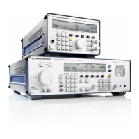
V L F > H F R E C E I V E R S
f
R & S E K 8 9 5 / R & S E K 8 9 6
User Manual
f
IF Processor GM 893 (Option)
1.3.14 IF Processor R&S GM 893 (Mod. 03 =Wideband Output, Option)
1.3.14.1 Design
The IF Processor R&S GM 893 (Mod. 03 = wide>
band output) consists of a printed circuit
board, a set of screens, two RF covers, two grey
extracting levers, the interface to the carrier
board as well as HF interfaces.
1.3.14.2 Functioning
(See Fig. 1.18)
The receive signal ANTIN (f > 500 kHz) from
the IF / AF processor is routed via a relay to a
transformer. The latter provides for signal level
matching, decouples the IF processor from the
preceding modules and splits up the receive
signal.
Part of the receive signal ANT OUT is fed to the
HF unit.
The transformer is connected via a lowpass fil>
ter to a converter stage.
The converter stage converts the receive signal
into the intermediate frequency of 41.44 MHz
by using the oscillator frequency variable in 1>
Hz increments from the synthesizer.
The 41.44>MHz signal is applied via a lowpass
filter to an active bandpass filter.
The bandpass filter is followed by an amplifier.
The latter works in common>base connection
and thus ensures a high HF gain and a large
bandwidth. The amplified signal WB OUT is
routed via an RF cable to interface OPTION.
The receive signal ANTIN (f e 500 kHz) from
the IF / AF processor is fed via a relay to the HF
unit.
1st OSC
Fig. 1.18 IF Processor R&S GM 893 (Mod. 03 = Wideband Output, Option),
Block Diagram
ANT
IN
ANT
OUT
LF
WBOUT
6164.0717.02_01
> 1.31 >

 Loading...