D.13
Date Code 20080918 Instruction Manual SEL-749M Relay
Modbus RTU Communications Protocol
Modbus Register Map
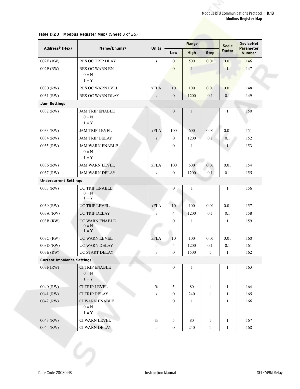
002E (RW) RES OC TRIP DLAY s 0 500 0.01 0.01 146
002F (RW) RES OC WARN EN
0 = N
1 = Y
01 1 147
0030 (RW) RES OC WARN LVLL xFLA 10 100 0.01 0.01 148
0031 (RW) RES OC WARN DLAY s 0 1200 0.1 0.1 149
Jam Settings
0032 (RW) JAM TRIP ENABLE
0 = N
1 = Y
01 1 150
0033 (RW) JAM TRIP LEVEL xFLA 100 600 0.01 0.01 151
0034 (RW) JAM TRIP DELAY s 0 1200 0.1 0.1 152
0035 (RW) JAM WARN ENABLE
0 = N
1 = Y
01 1 153
0036 (RW) JAM WARN LEVEL xFLA 100 600 0.01 0.01 154
0037 (RW) JAM WARN DELAY s 0 1200 0.1 0.1 155
Undercurrent Settings
0038 (RW) UC TRIP ENABLE
0 = N
1 = Y
01 1 156
0039 (RW) UC TRIP LEVEL xFLA 10 100 0.01 0.01 157
003A (RW) UC TRIP DELAY s 4 1200 0.1 0.1 158
003B (RW) UC WARN ENABLE
0 = N
1 = Y
01 1 159
003C (RW) UC WARN LEVEL xFLA 10 100 0.01 0.01 160
003D (RW) UC WARN DELAY s 4 1200 0.1 0.1 161
003E (RW) UC START DELAY s 0 1500 1 1 162
Current Imbalance Settings
003F (RW) CI TRIP ENABLE
0 = N
1 = Y
01 1 163
0040 (RW) CI TRIP LEVEL % 5 80 1 1 164
0041 (RW) CI TRIP DELAY s 0 240 1 1 165
0042 (RW) CI WARN ENABLE
0 = N
1 = Y
01 1 166
0043 (RW) CI WARN LEVEL % 5 80 1 1 167
0044 (RW) CI WARN DELAY s 0 240 1 1 168
Table D.23 Modbus Register Map
a
(Sheet 3 of 26)
Address
b
(Hex) Name/Enums
c
Units
Range
Scale
Fa c tor
DeviceNet
Parameter
Number
Low High Step
Courtesy of NationalSwitchgear.com
 Loading...