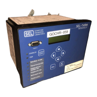
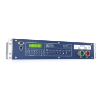
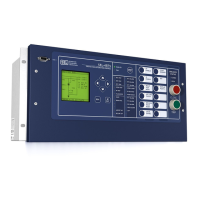
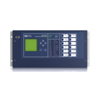
Date Code 20080918 Instruction Manual SEL-749M Relay
List of Tables
R.Instruc tion Manual
Table 1.1 SEL-749M Serial Port Settings.............................................................................................. 1.6
Table 2.1 Slot Allocations for Different Cards ...................................................................................... 2.2
Table 2.2 Communications Ports ........................................................................................................... 2.3
Table 2.3 Communications Card Interfaces and Connectors................................................................. 2.4
Table 2.4 Voltage Card Terminal Designation .......................................................................................2.4
Table 2.5 Current Card Terminal Designation .......................................................................................2.5
Table 2.6 I/O Card (3 DI/4 DO/1 AO) Terminal Allocation .................................................................. 2.5
Table 2.7 I/O Card (8 DI) Terminal Allocation......................................................................................2.5
Table 2.8 PTC Cable Requirements ..................................................................................................... 2.12
Table 2.9 Wire-Size Guide ................................................................................................................... 2.13
Table 3.1 SEL Software Solutions ......................................................................................................... 3.1
Table 3.2
ACSELERATOR QuickSet SEL-5030 Software....................................................................... 3.1
Table 3.3 File/Tools Menus.................................................................................................................... 3.6
Table 3.4
ACSELERATOR QuickSet Help Forms.................................................................................. 3.14
Table 4.1 Identifier Settings ................................................................................................................... 4.3
Table 4.2 CT Configuration and Full Load Current Settings................................................................. 4.3
Table 4.3 Voltage Settings...................................................................................................................... 4.3
Table 4.4 Overload (Thermal Model) Settings ...................................................................................... 4.5
Table 4.5 Thermal Limit Tripping Times in Seconds vs. Multiples of Full-Load Amps
(Service Factor = 1.01).......................................................................................................... 4.8
Table 4.6 Overload Settings (Alarm, Start Inhibit, Cooling, and RTD Bias)......................................... 4.9
Table 4.7 Phase Overcurrent Settings .................................................................................................. 4.10
Table 4.8 Neutral Overcurrent Settings................................................................................................ 4.11
Table 4.9 Residual Overcurrent Settings.............................................................................................. 4.13
Table 4.10 Load Jam Settings ................................................................................................................ 4.13
Table 4.11 Undercurrent Settings........................................................................................................... 4.14
Table 4.12 Current Imbalance Settings .................................................................................................. 4.15
Table 4.13 Protection Disable Settings .................................................................................................. 4.16
Table 4.14 Start Monitor Settings .......................................................................................................... 4.16
Table 4.15 Star-Delta Settings................................................................................................................ 4.17
Table 4.16 Start Inhibit Settings............................................................................................................. 4.17
Table 4.17 Phase Reversal Setting ......................................................................................................... 4.18
Table 4.18 Speed Switch Settings .......................................................................................................... 4.20
Table 4.19 PTC Settings......................................................................................................................... 4.20
Table 4.20 RTD Settings ........................................................................................................................ 4.21
Table 4.21 Undervoltage Settings .......................................................................................................... 4.24
Table 4.22 Overvoltage Settings ............................................................................................................ 4.24
Table 4.23 VAR Settings ........................................................................................................................ 4.26
Table 4.24 Underpower Settings ............................................................................................................ 4.26
Table 4.25 Power Factor Settings........................................................................................................... 4.27
Table 4.26 Frequency Settings ............................................................................................................... 4.30
Table 4.27 Load Control Settings........................................................................................................... 4.31
Table 4.28 Analog Output Setting.......................................................................................................... 4.31
Table 4.29 Scaling of Analog Output..................................................................................................... 4.32
Table 4.30 Trip Inhibit Settings.............................................................................................................. 4.32
Table 4.31 Trip and Close Logic Settings .............................................................................................. 4.33
Table 4.32 Motor Control Settings......................................................................................................... 4.36
Table 4.33 Settings Selected by SPEED2 Input..................................................................................... 4.38
Table 4.34 SEL
OGIC Enable Settings ..................................................................................................... 4.38
Table 4.35 Latch Bits Equations Settings .............................................................................................. 4.38
Table 4.36 SEL
OGIC Variable/Timer Settings........................................................................................ 4.39
Table 4.37 Control Output Equations and Contact Behavior Settings................................................... 4.39
Table 4.38 General Global Settings ....................................................................................................... 4.40
Table 4.39 Target Reset Setting.............................................................................................................. 4.40
Courtesy of NationalSwitchgear.com