1.6
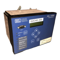
SEL-749M Relay Instruction Manual Date Code 20080918
Introduction and Specifications
Getting Started
=>QUIT <Enter>
Motor 1 Date: 12/10/2003 Time: 10:31:43.797
Station 1
Figure 1.1 Response Header
Checking
Relay Status
Use the STA serial port command to view the SEL-749M operational status.
Analog channel dc offset and monitored component status are listed in the
status report depicted in Figure 1.2.
=>>STA <Enter>
SEL-749M Date: 12/10/2003 Time: 18:17:34.442
MOTOR RELAY Time Source: internal
FID=SEL-749M-R100-V0-Z001001-D20031210 CID=0965
Part Number 0749M01B610X0X11
SELF TESTS
Current IA IB IC IN
Offset: OK/WARN OK/WARN OK/WARN OK/WARN
Voltage VA VB VC
Offset: OK/WARN OK/WARN OK/WARN
PS_Vdc FPGA GPSB HMI
OK/FAIL OK/FAIL OK/FAIL OK/WARN
RAM ROM CR_RAM Non_Vol Clk_Bat Clock
OK/FAIL OK/FAIL OKFAIL OK/FAIL OK/WARN OK/WARN
PTC RTD Current Voltage I/O_Crd
OK/FAIL OK/FAIL OK/FAIL OK/FAIL OK/FAIL
Relay Enabled/Disabled
Figure 1.2 STA Command Response—No Communications Card or
Communications Card/Modbus RTU Protocol
If a communications card with DeviceNet protocol is present, then the status
report depicted in Figure 1.3 applies.
=>>STA <Enter>
SEL-749M Date: 12/10/2003 Time: 19:10:13.221
MOTOR RELAY Time Source: internal
FID=SEL-749M-R100-V0-Z001001-D20031210 CID=0965
Part Number 0749M01B613X0X11
SELF TESTS
Current IA IB IC IN
Offset: OK/WARN OK/WARN OK/WARN OK/WARN
Voltage VA VB VC
Offset: OK/WARN OK/WARN OK/WARN
PS_Vdc FPGA GPSB HMI
OK/FAIL OK/FAIL OK/FAIL OK/WARN
RAM ROM CR_RAM Non_Vol Clk_Bat Clock
OK/FAIL OK/FAIL OKFAIL OK/FAIL OK/WARN OK/WARN
PTC RTD Current Voltage I/O_Crd COM_Crd
OK/FAIL OK/FAIL OK/FAIL OK/FAIL OK/FAIL OK/FAIL
MAC_ID ASA DN_Rate DN_Status
Dd nnn nnnnh ___kbps 000b bbbb
Relay Enabled/Disabled
Figure 1.3 STA Command Response—Communications Card/DeviceNet
Protocol
Table 1.1 SEL-749M Serial Port Settings
Description Setting Label Default Value
SPEED SPEED 9600
DATA BITS BITS 8
PARITY PARITY N
STOP BITS STOP 1
PORT TIMEOUT T_OUT 15
HDWR HANDSHAKING RTSCTS N
Courtesy of NationalSwitchgear.com