AG7 module theory of operation
AG7 module the
ory of operation
This section
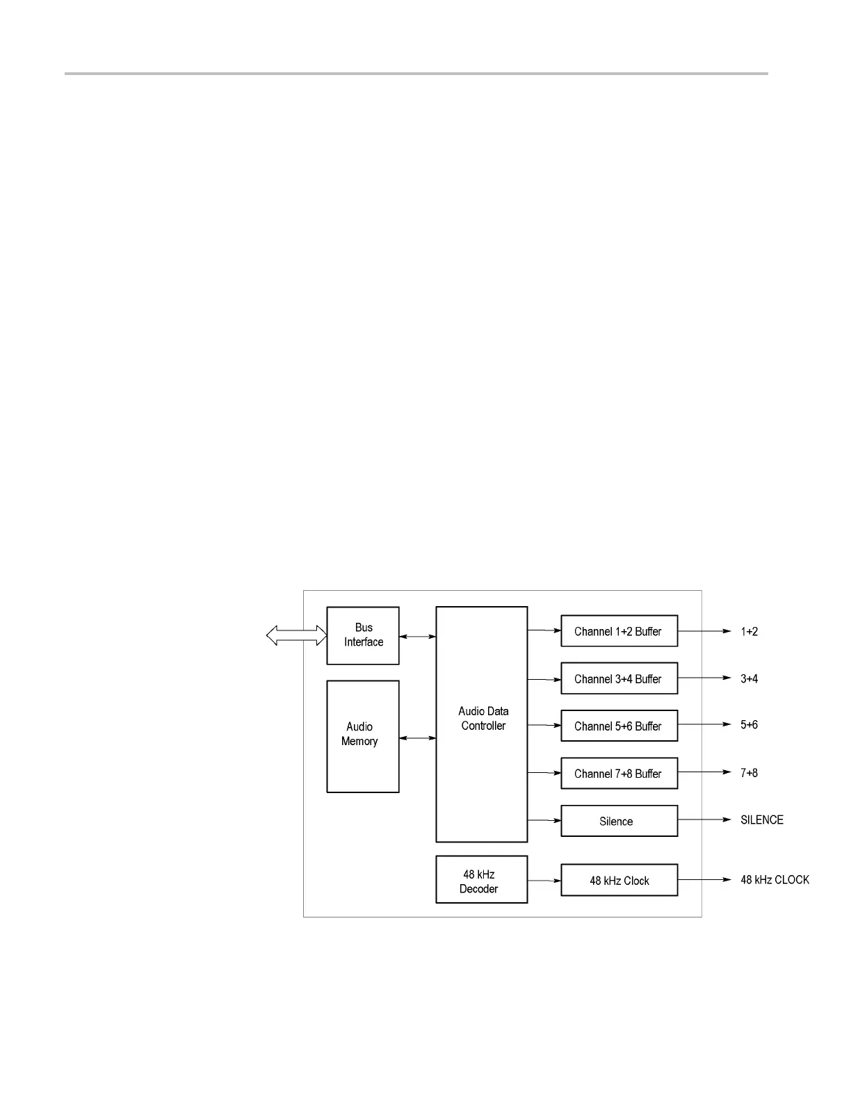
describes the basic operation of the major circuit blocks in the AG7
Audio Generator module.
Bus interface
This block provides the communication between the mainframe and the module
circuit.
Audio memory
This block contains 20/24 bits audio data for all of the serial audio outputs.
Audio data con troller and
48 kHz dec
oder
The block is a part of the FPGA. It receives audio data from the Audio Memory
and encod
es these data to serial audio data stream that comply with the AES/EBU
standard. It also generates 48 kHz clock signal.
Channel buffers (1+2, 3+4,
5+6, 7+8
, and silence)
These blocks receive the digital audio data from the FPGA and set the output
amplit
ude to the specified level.
48 kHz clock buffer
The block outputs 48 kHz clock signal. The output level of the clock signal can be
set to either a CMOS compatible level or 1 V. This feature is available through
jumpe
r J452 on the circuit board.
Figure 3-1: Simplified block diagram of the AG7 module
3–2 TG8000 Multiformat Test Signal Generator Service Manual
 Loading...