1
3
5
7
9
11
13
2
4
6
8
10
12
14
TEST/SBWTCK
MSP430Fxxx
RST/NMI/SBWTDIO
TDO/TDI
TCK
GND
TEST/VPP
JTAG
VCC TOOL
VCC TARGET
330Ω
R2
J1 (see Note A)
J2 (see Note A)
Important to connect
V /AV /DV
CCCC CC
V /AV /DV
SS SS SS
R1
47 kΩ
C1
2.2 nF
(See Note B)
V
CC
C2
10 µF
C3
0.1 µF
www.ti.com
Signal Connections for In-System Programming and Debugging
23
SLAU278Y–May 2009–Revised March 2016
Submit Documentation Feedback
Copyright © 2009–2016, Texas Instruments Incorporated
Design Considerations for In-Circuit Programming
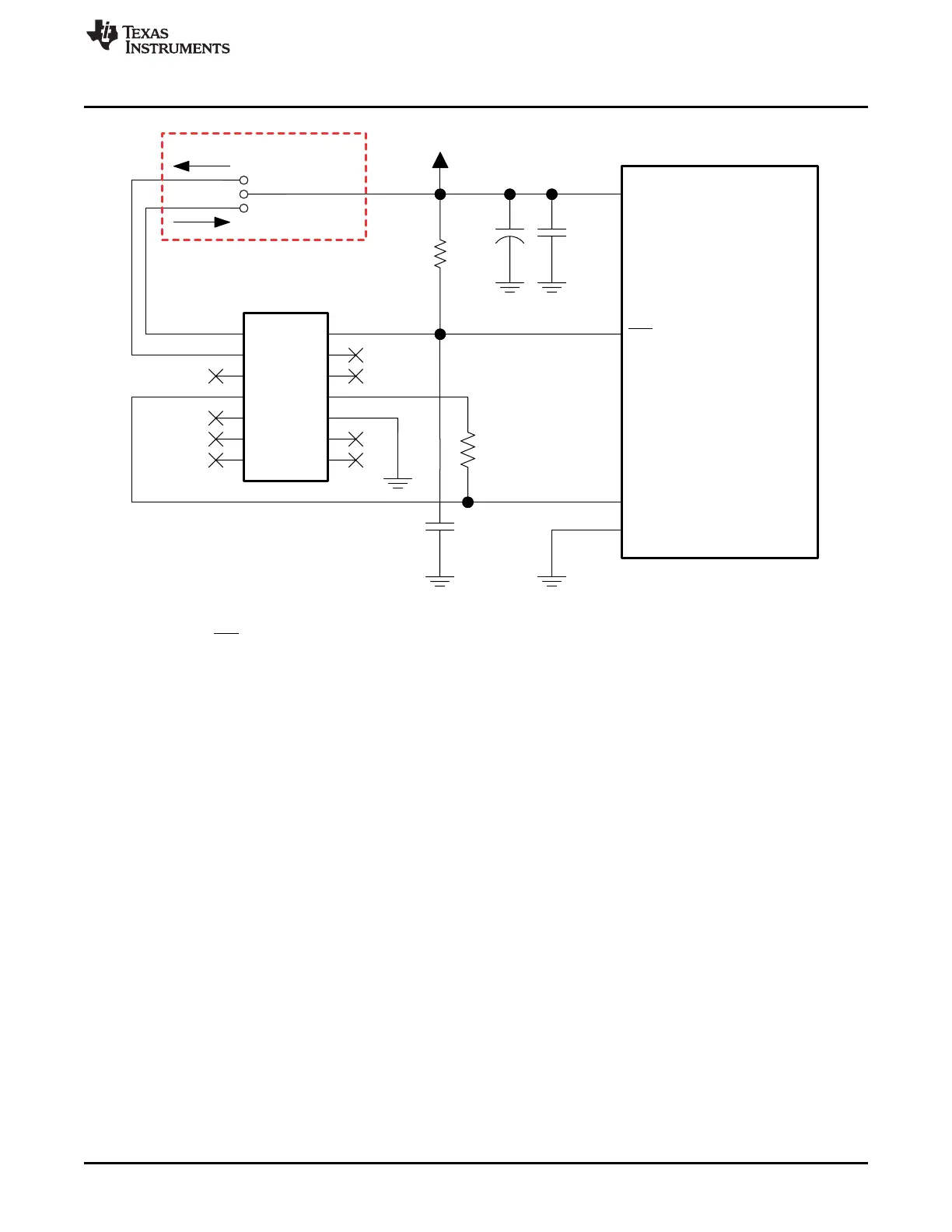
A If a local target power supply is used, make connection J1. If power from the debug or programming adapter is used,
make connection J2.
B The device RST/NMI/SBWTDIO pin is used in 2-wire mode for bidirectional communication with the device during
JTAG access, and any capacitance that is attached to this signal may affect the ability to establish a connection with
the device. The upper limit for C1 is 2.2 nF when using current TI tools.
Some EVMs use a value of 1.1 nF to enable high-speed SBW communication.
C R2 protects the JTAG debug interface TCK signal from the JTAG security fuse blow voltage that is supplied by the
TEST/VPP pin during the fuse blow process. If fuse blow functionality is not needed, R2 is not required (populate 0 Ω)
and do not connect TEST/VPP to TEST/SBWTCK.
Figure 2-2. Signal Connections for 2-Wire JTAG Communication (Spy-Bi-Wire) Used by MSP430F2xx,
MSP430G2xx, and MSP430F4xx Devices