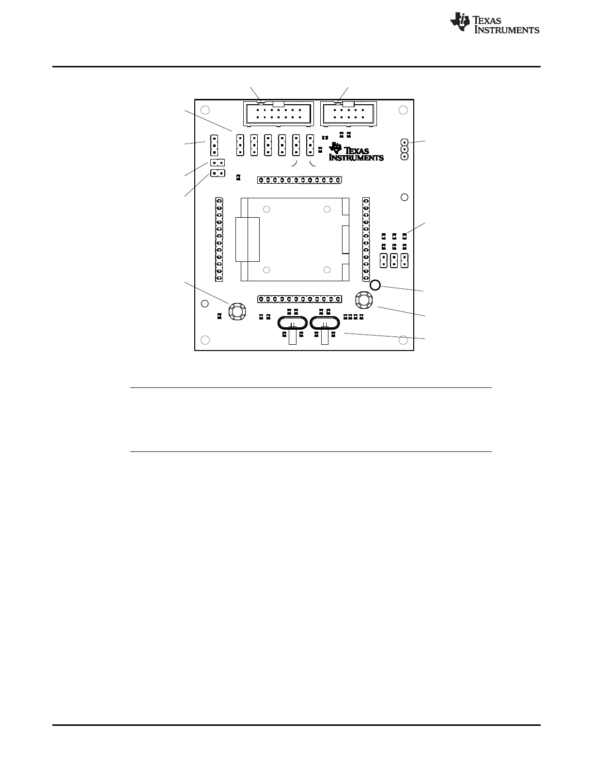
Jumper JP1
Open to measure current
Connector J2
External power connector
Jumper J1 to "ext"
Jumpers JP3 to JP8
Close 1-2 to debug in Spy-Bi-Wire mode
Close 2-3 to debug in 4-wire JTAG mode
Switch SW1
Device reset
LEDs connected to
P1.0, P1.1, P1.2 via
JP9, JP10, JP11
(only D1 assembled)
Orient Pin 1 of MSP430 device
Connector JTAG
For JTAG Tool
Connector BOOTST
For ToolBootloader
Jumper J1
1-2 (int): Power supply from JTAG interface
2-3 (ext): External power supply
Jumper JP2
Analog/digital power
Switch SW2
Connected to P1.3
HF ands LF oscillators with capacitors
and resistors to connect pinheads
1
Vcc
ext
int
Vcc
GND
GND
JTAG
SBW
5
10
1520
25
30
35
40
45
RESET
Ext.
Pwr.
PWR
DVCC
AVCC
TCK TMS TDI TDO
RST/SBWTDIO
TEST/SBWTCK
GND
GND
P1.3
14
1
2
10
1
2
1 2 3
123
123
123
123
123
123
QFN11T048-008 A101121
Clamshell
MSP-TS430RGZ48C
Rev. 1.2 RoHS
Q2
Q1
P1.0
P1.1
P1.2
JTAG
C2
C1
C4
R1
BOOTST
R2
R3
J2
J1
JP1
JP9
C5
R4
JP3
JP4
JP5
JP6JP7
JP8
R5
R6
R7
C3
C6
C7
D1
R10
JP10
D2
R11
JP11
D3
R12
JP2
C8
C9
R8
R9
U1
SW1
R13
TP2
TP1
SW2
R14
MSP-TS430RGZ48C
www.ti.com
86
SLAU278Y–May 2009–Revised March 2016
Submit Documentation Feedback
Copyright © 2009–2016, Texas Instruments Incorporated
Hardware
Figure B-37. MSP-TS430RGZ48C Target Socket Module, PCB
NOTE: LFOSC and HFOSC pins are swapped at SV1.
42_HFXIN (pin 42) → SV1 (pin 7)
43_HFXOUT (pin 43) → SV1 (pin 6)
45_LFXIN (pin 45) → SV1 (pin 10)
46_LFXOUT (pin 46) → SV1 (pin 9)