1
3
5
7
9
11
13
2
4
6
8
10
12
14
TDO/TDI
TDI/VPP
TMS
TCK
GND
TEST/VPP
JTAG
VCC TOOL
VCC TARGET
J1 (see Note A)
J2 (see Note A)
V
CC
R1
47 k
(see Note B)
W
C2
10 µF
C3
0.1 µF
V /AV /DV
CCCC CC
RST/NMI
TDO/TDI
TDI/VPP
TMS
TCK
TEST/VPP (see Note C)
V /AV /DV
SS SS SS
MSP430Fxxx
C1
10 nF/2.2 nF
(see Notes B and E)
RST (see Note D)
Important to connect
Signal Connections for In-System Programming and Debugging
www.ti.com
22
SLAU278Y–May 2009–Revised March 2016
Submit Documentation Feedback
Copyright © 2009–2016, Texas Instruments Incorporated
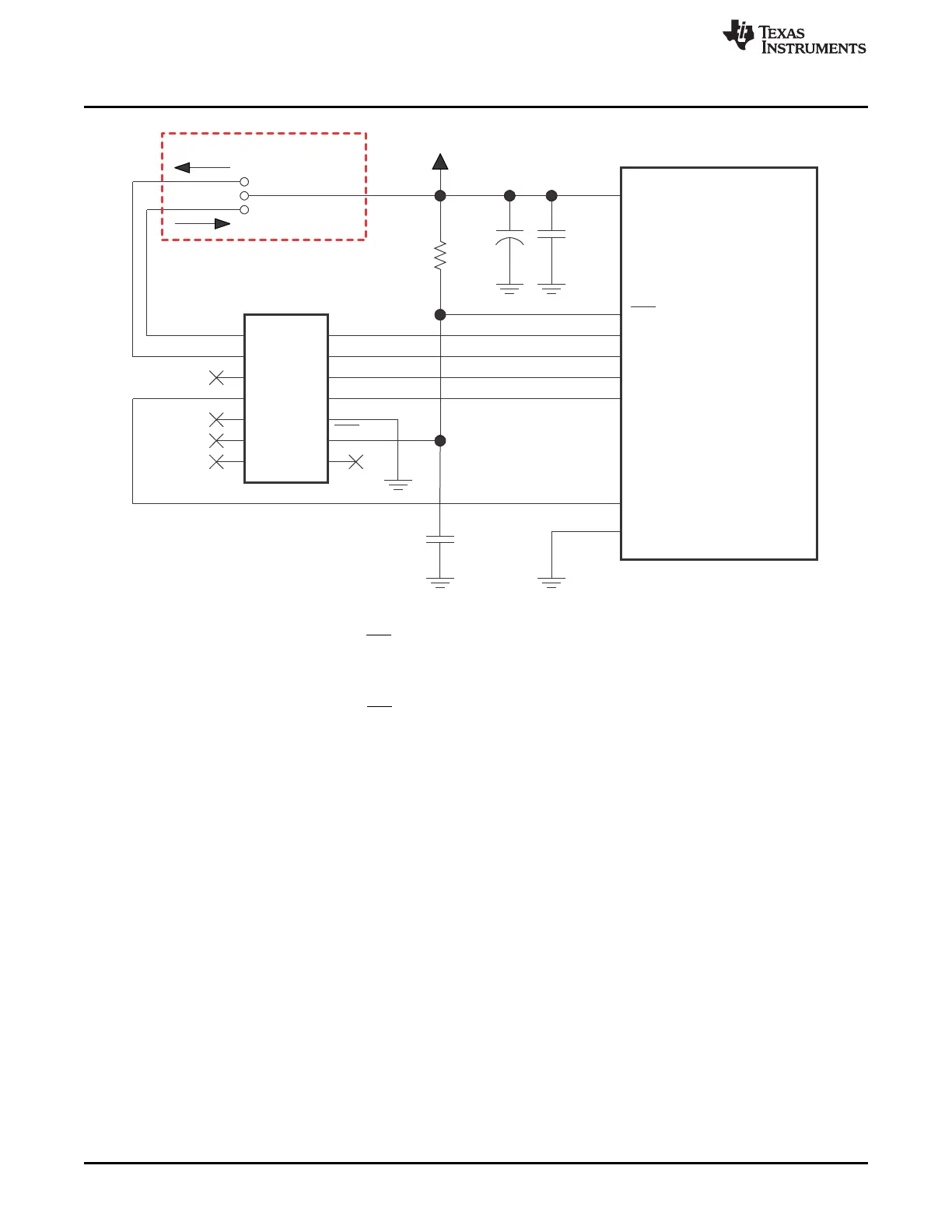
Design Considerations for In-Circuit Programming
A If a local target power supply is used, make connection J1. If power from the debug or programming adapter is used,
make connection J2.
B The configuration of R1 and C1 for the RST/NMI pin depends on the device family. See the respective MSP430 family
user's guide for the recommended configuration.
C The TEST pin is available only on MSP430 family members with multiplexed JTAG pins. See the device-specific data
sheet to determine if this pin is available.
D The connection to the JTAG connector RST pin is required when programming or debugging a device that supports
2-wire JTAG communication, even when using 4-wire JTAG communication mode on these devices. However, this
connection is optional on devices that do not support 2-wire JTAG communication.
E When using a device that supports 2-wire JTAG communication in 4-wire JTAG mode, the upper limit for C1 should
not exceed 2.2 nF. This applies to both TI FET interface modules (LPT and USB FET).
Some EVMs use a value of 1.1 nF to enable high-speed SBW communication.
Figure 2-1. Signal Connections for 4-Wire JTAG Communication