52 www.xilinx.com Virtex-4 FPGA Configuration User Guide
UG071 (v1.12) June 2, 2017
Chapter 2: Configuration Interfaces
SelectMAP Data Ordering
In many cases, SelectMAP configuration is driven by a user application residing on a
microprocessor, CPLD, or in some cases another FPGA. In these applications, it is
important to understand how the data ordering in the configuration data file corresponds
to the data ordering expected by the FPGA.
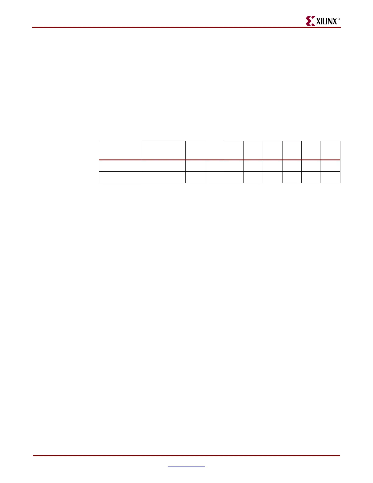
In SelectMAP 8-bit mode, configuration data is loaded at one byte per CCLK, with the MSB
of each byte presented to the D0 pin. This convention (D0 = MSB, D7 = LSB) differs from
many other devices. This can be a source of confusion when designing custom
configuration solutions. Table 2-6 shows how to load the hexadecimal value 0xABCD into
the SelectMAP data bus.
Some applications can accommodate the non-conventional data ordering without
difficulty. For other applications, it can be more convenient for the source configuration
data file to be byte-swapped, meaning that the bits in each byte of the data stream are
reversed. For these applications, the Xilinx PROM file generation software can generate
byte-swapped PROM files (see “Configuration Data Files”).
In SelectMAP 32-bit mode, configuring the data order is straight D0 = LSB and D31 = MSB.
Table 2-6: Bit Ordering for SelectMAP 8-bit Mode
CCLK Cycle
Hex
Equivalent
D0 D1 D2 D3 D4 D5 D6 D7
1 0xAB 1 0 1 0 1 0 1 1
2 0xCD 1 1 0 0 1 1 0 1
Notes:
1. D[0:7] represent the SelectMAP 8-bit mode data pins.

 Loading...


