Virtex-4 FPGA Configuration User Guide www.xilinx.com 83
UG071 (v1.12) June 2, 2017
Dynamic Reconfiguration of Functional Blocks (DRP)
DRP DCM Implementation
The DRP implementation allows dynamic adjustment of M, D, and PS values (direct mode)
in the DCM. The following ports are available in DCM_ADV primitive (see Chapter 2 of
the Virtex-4 FPGA User Guide):
Inputs:
DI[15:0]
DADDR[6:0]
DWE
DEN
DCLK
Outputs:
DO[15:0]
DRDY
DADDR[6:0] is latched at DCLK rising edge while DEN is asserted. The DO output reflects
the status of that latched address location. After reset, the internal address is reset to 0, and
the DCM DRP DO outputs are used to signal the default status Phase Shift Overflow,
CLKIN Stopped, CLKFX Stopped, and CLKFB Stopped. However, if the DRP is used to
reprogram M, D, or PS value, the DO is no longer showing default status. To access default
status, the user must perform a DRP read with DADDR[6:0] = 0.
Changing the Multiply and Divide Values
The Multiply and Divide (M/D) values can be directly programmed in the DCM through
the DRP by writing to hex addresses 50h and 52h respectively. The five least-significant
data bits represent the multiply-minus-1 and divide-minus-1 values, as shown in Table 6-2
and Table 6-3. DRDY indicates that the new value has been written successfully.
The DCM must be held in reset by activating input RST while changing the M/D values.
At some point after RST is released, signal LOCKED goes true, indicating that the clock
outputs of the DCM are valid.
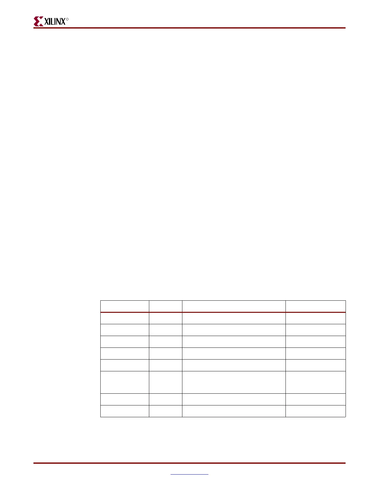
Table 6-2: Multiplier Settings
DADDR[15:0] DEC DI[15:0] Function
50h 0000 0000h (0000000000000000) N/A
50h 0001 0001h (0000000000000001) Multiply by 2
50h 0002 0002h (0000000000000010) Multiply by 3
50h 0003 0003h (0000000000000011) Multiply by 4
50h 0004 0004h (0000000000000100) Multiply by 5
•
•
•
•
•
•
•
•
•
•
•
•
50h 0030 001Eh (0000000000011110) Multiply by 31
50h 0031 001Fh (0000000000011111) Multiply by 32

 Loading...


