Virtex-4 FPGA Configuration User Guide www.xilinx.com 29
UG071 (v1.12) June 2, 2017
Serial Configuration Interface
Clocking Serial Configuration Data
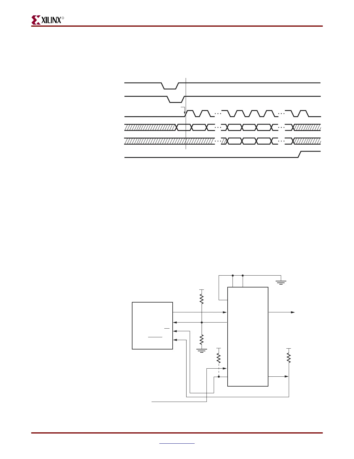
Figure 2-2 shows how configuration data are clocked into Virtex-4 devices in Slave serial
and Master serial modes.
Notes relevant to Figure 2-2:
1. In Figure 2-2, bit 0 represents the MSB of the first byte. For example, if the first byte is
0xAA (1010_1010), bit 0=1, bit 1=0, bit 2=1, etc.
2. For Master configuration mode, CCLK does not transition until after MODE pins are
sampled, as indicated by the arrow.
3. CCLK can be free-running in Slave serial mode.
Master Serial Configuration
The Master serial mode is designed so that the FPGA can be configured from a
Xilinx® serial configuration PROM, as shown in Figure 2-3.
Figure 2-2: Serial Daisy Chain Configuration Clocking Sequence
PROGRAM_B
INIT_B
CCLK
DONE
Master DIN
Master CLK Begins Here
(2)
Data bits clocked on rising edge of CCLK
ug071_016_073007
BIT 0
(1)
BIT 1 BIT n BIT n+1
BIT n-63BIT n-64
Master DOUT /
Slave DIN
Figure 2-3: Master Serial Mode Configuration
Xilinx
Serial PROM
Virtex-4
Master
Serial
DATA DOUT
INIT_B
DIN
CCLK
PROGRAM_B
DONE
M2
M0 M1
CLK
CE
RESET/OE
PROGRAM_B
UG071_12_073007
(2)(1)
(7)
(7)

 Loading...


