106 www.xilinx.com Virtex-4 FPGA Configuration User Guide
UG071 (v1.12) June 2, 2017
Chapter 8: Readback and Configuration Verification
The packets shifted in to the JTAG CFG_IN register are identical to the packets shifted in
through the SelectMAP interface when reading the STAT register through SelectMAP.
Configuration Memory Read Procedure (1149.1 JTAG)
The process for reading configuration memory from the FDRO register through the JTAG
interface is similar to the process for reading from other registers. However, additional
steps are needed to accommodate frame logic. Configuration data coming from the FDRO
register pass through the frame buffer, therefore the first frame of readback data is dummy
data and should be discarded (refer to the FDRI and FDRO register description). The 1149.1
JTAG readback flow is recommended for most users.
1. Reset the TAP controller.
2. Shift the CFG_IN instruction into the JTAG Instruction Register. The LSB of the
CFG_IN instruction is shifted first; the MSB is shifted while moving the TAP controller
out of the SHIFT-IR state.
3. Shift packet write commands into the CFG_IN register through the Shift-DR state:
a. Write a dummy word to the device.
b. Write the Synchronization word to the device.
c. Write a NOOP instruction to the device.
d. Write the RCRC command to the device.
e. Write two dummy words to flush the packet buffer.
4. Shift the JSHUTDOWN instruction into the JTAG Instruction Register.
5. Move into the RTI state; remain there for 12 TCK cycles to complete the Shutdown
sequence. The DONE pin goes Low during the Shutdown sequence.
6. Shift the CFG_IN instruction into the JTAG Instruction Register.
7. Move to the Shift-DR state and shift packet write commands into the CFG_IN register:
a. Write a dummy word to the device.
b. Write the Synchronization word to the device.
c. Write a NOOP instruction to the device.
d. Write the write CMD register header.
e. Write the RCFG command to the device.
f. Write the write FAR register header.
g. Write the starting frame address to the FAR register (typically 0x0000000).
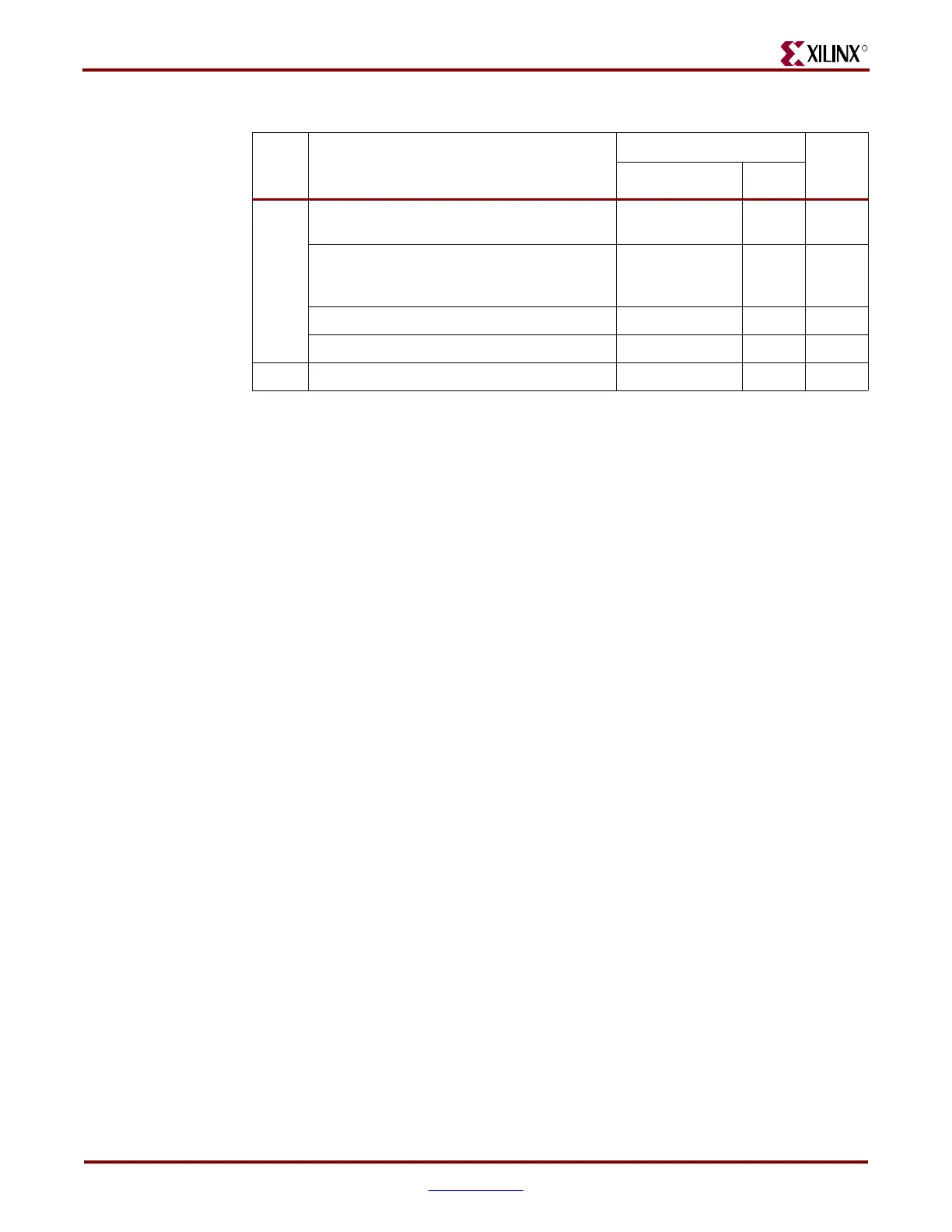
5
Shift the contents of the STAT register out of the
CFG_OUT data register.
0xSSSSSSSS 031
Shift the last bit of the STAT register out of the
CFG_OUT data register while exiting
SHIFT-DR.
S11
Move into the Select-IR state. X 1 3
Move into the Shift-IR State. X 0 2
6 Reset the TAP Controller. X 1 5
Table 8-4: Status Register Readback Command Sequence (JTAG) (Continued)
Step Description
Set and Hold # of
Clocks
(TCK)
TDI TMS

 Loading...


