62 www.xilinx.com Virtex-4 FPGA Configuration User Guide
UG071 (v1.12) June 2, 2017
Chapter 3: Boundary-Scan and JTAG Configuration
Bit Sequence Boundary-Scan Register
The order of each non-TAP IOB is described in this section. The input is first, then the
output, and finally the 3-state IOB control. The 3-state IOB control is closest to the TDO.
The input-only pins contribute only the input bit to the Boundary-Scan I/O data register.
The bit sequence of the device is obtainable from the Boundary-Scan Description Language
Files (BSDL files) for the Virtex-4 family. (These files can be obtained from the Xilinx
software download area.) The bit sequence always has the same bit order and the same
number of bits, and is independent of the design.
Instruction Register
The Instruction Register (IR) for the Virtex-4 device is connected between TDI and TDO
during an instruction scan sequence. In preparation for an instruction scan sequence, the
instruction register is parallel-loaded with a fixed instruction capture pattern. This pattern
is shifted out onto TDO (LSB first), while an instruction is shifted into the instruction
register from TDI.
To determine the operation to be invoked, an OPCODE necessary for the Virtex-4
Boundary-Scan instruction set is loaded into the Instruction Register. The length of the IR
is device size-specific. The IR is 10 bits wide for all Virtex-4 LX, SX, and single-processor FX
devices. FX devices with two processors have a 14-bit IR. The bottom six bits of the
instruction codes are the same for all devices sizes to support the new IEEE Standard 1532
for In-System Configurable (ISC) devices. The additional IR bits for each instruction are 1s.
Table 3-3 lists the available instructions for Virtex-4 devices. Figure 3-4 shows the
instruction capture values loaded into the IR as part of an instruction scan sequence.
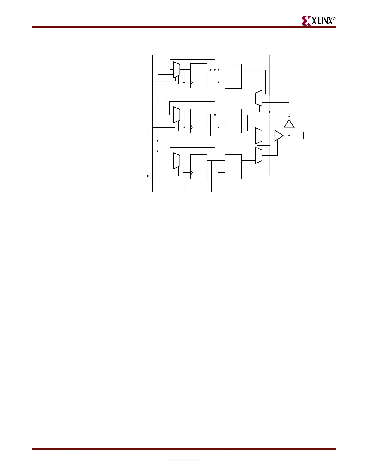
Figure 3-3: Virtex-4 Family Boundary-Scan Logic
D Q
1
0
1x
01
00
1x
01
00
1x
01
00
D Q
D Q
1
0
1
0
DQ
LE
sd
sd
LE
DQ
sd
LE
DQ
TDI
IOB.I
INTEST
IOB.O
IOB.T
EXTEST
SHIFT CLOCK DATA
REGISTER
TDO UPDATE INTEST is OR'd with EXTEST
ug071_39_121703

 Loading...


