66 www.xilinx.com Virtex-4 FPGA Configuration User Guide
UG071 (v1.12) June 2, 2017
Chapter 3: Boundary-Scan and JTAG Configuration
Configuration Register (Boundary-Scan)
The configuration register is a 64-bit register. This register allows access to the
configuration bus and readback operations.
USERCODE Register
The USERCODE instruction is supported in the Virtex-4 family. This register allows a user
to specify a design-specific identification code. The USERCODE can be programmed into
the device and can be read back for verification later. The USERCODE is embedded into
the bitstream during bitstream generation (BitGen -g UserID option) and is valid only
after configuration. If the device is blank or the USERCODE was not programmed, the
USERCODE register contains 0xFFFFFFFF.
USER1, USER2, USER3, and USER4 Registers
The USER1, USER2, USER3, and USER4 registers are only available after configuration.
These four registers must be defined by the user within the design. These registers can be
accessed after they are defined by the TAP pins.
The BSCAN_VIRTEX4 library macro is required when creating these registers. This symbol
is only required for driving internal scan chains (USER1, USER2, USER3, and USER4).
A common input pin (TDI) and shared output pins represent the state of the TAP controller
(RESET, SHIFT, and UPDATE). Unlike earlier FPGA families that required the BSCAN
macro to dedicate TAP pins for Boundary-Scan, Virtex-4 TAP pins are dedicated and do
not require the BSCAN_VIRTEX4 macro for normal Boundary-Scan instructions or
operations. For HDL, the BSCAN_VIRTEX4 macro must be instantiated in the design.
Using Boundary-Scan in Virtex-4 Devices
Characterization data for some of the most commonly requested timing parameters shown
in Figure 3-5 are listed in the Virtex-4 FPGA Data Sheet in the Configuration Switching
Characteristics table.
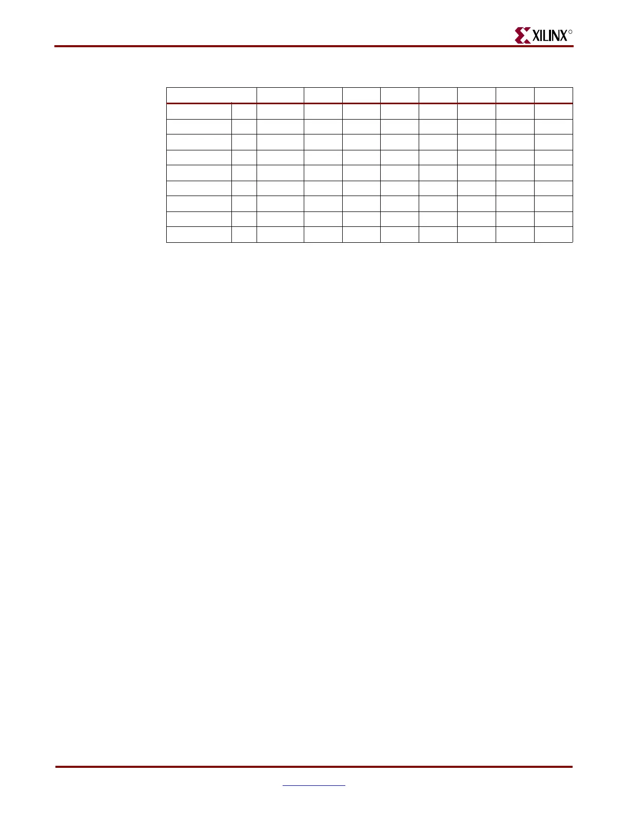
hex <v>1E64093
XC4VFX40
(1)
bin <vvvv> 0001 1110 1001 0100 0000 1001 0011
hex <v>1E8C093
XC4VFX60 bin <vvvv> 0001 1110 1011 0100 0000 1001 0011
hex <v>1EB4093
XC4VFX100 bin <vvvv> 0001 1110 1110 0100 0000 1001 0011
hex <v>1EE4093
XC4VFX140 bin <vvvv> 0001 1111 0001 0100 0000 1001 0011
hex <v>1F14093
Notes:
1. Does not reflect the actual device array size.
Table 3-5: Example JTAG IDCODE Concatenation (Continued)
vvvv ffff fffa aaaa aaaa cccc cccc ccc1

 Loading...


