Virtex-4 FPGA Configuration User Guide www.xilinx.com 13
UG071 (v1.12) June 2, 2017
Chapter 1
Configuration Overview
Introduction
Virtex®-4 devices are configured by loading application-specific configuration data—the
bitstream—into internal memory. Because Xilinx® FPGA configuration memory is
volatile, it must be configured each time it is powered-up. The bitstream is loaded into the
device through special configuration pins. These configuration pins serve as the interface
for a number of different configuration modes:
• Master-serial configuration mode
• Slave-serial configuration mode
• Master SelectMAP (parallel) configuration mode
• Slave SelectMAP (parallel) configuration mode
In addition, the bitstream can be loaded through the JTAG interface:
• JTAG/Boundary-Scan configuration mode
The configuration modes are explained in detail in Chapter 2 The configuration mode is
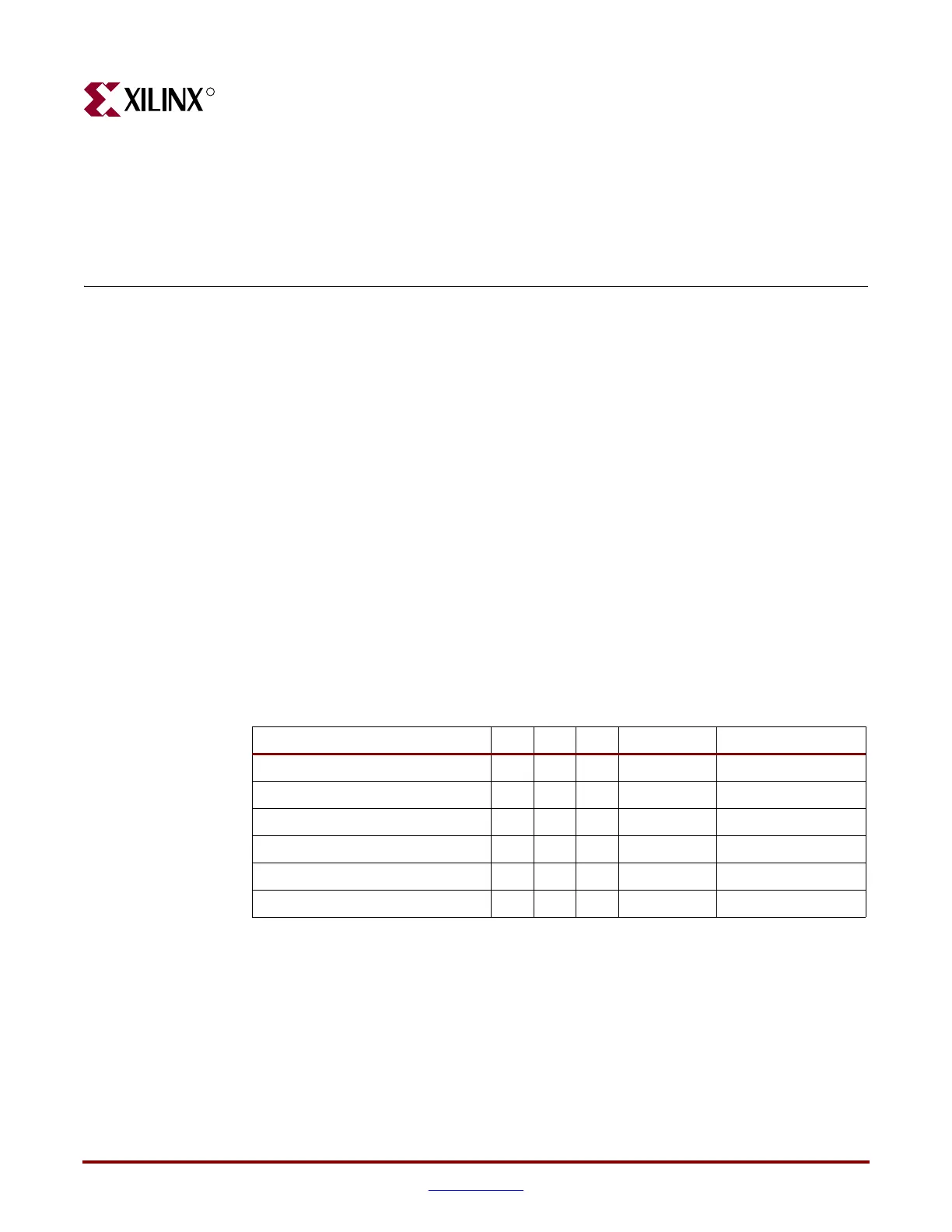
selected by setting the appropriate level on the dedicated MODE input pins. Table 1-1 lists
the Virtex-4 configuration modes.
Table 1-1: Virtex-4 Configuration Modes
Configuration Mode M2 M1 M0 Data Width CCLK Direction
Master Serial 000 1 bit Output
Slave Serial 111 1 bit Input
Master SelectMAP 011 8 bits Output
Slave SelectMAP8 110 8 bits Input
Slave SelectMAP32
(3)
001 32 bits Input
JTAG/Boundary-Scan only
(1)
101 1 bit –
Notes:
1. JTAG configuration uses the JTAG TCK pin instead of the configuration clock (CCLK).
2. I/O pre-configuration pull-up resistors are disabled with the HSWAPEN pin.
3. In SelectMAP32 D0:D31 data bits are not swapped. D0 is the LSB. D31 is the MSB.
4. If the pins are left unconnected a weak pull-up resistor on the mode pins makes slave serial the default
mode.

 Loading...


