84 www.xilinx.com Virtex-4 FPGA Configuration User Guide
UG071 (v1.12) June 2, 2017
Chapter 6: Reconfiguration Techniques
If the M or D values are dynamically charged, then in some cases, the frequency mode
must also be charged to comply with the specifications in the data sheet. For the
DFS_FREQUENCY_MODE DRP address, 41h must be read and bit 6 (DI[5]) is then set to:
• 0 for low frequency mode
• 1 for high frequency mode
All other bits must remain unchanged.
For the DLL_FREQUENCY_MODE DRP address, 58h must be read and bits 7 and 8
(DI[7:6) are then set to:
• 0 for low frequency mode
• 1 for high frequency mode
Again, all other bits must be left undisturbed.
Dynamic Phase Shifting Through the DRP in Direct Mode
In addition to the phase shift modes already available in Virtex-II and Virtex-II Pro devices,
the Virtex-4 FPGA has implemented a Direct Phase Shift Mode (DPSM). This allows the
user to control the phase-shift delay line elements (tabs) directly. The DPSM can be
accessed through either the standard Phase Shift (PS) interface or the DRP. If the DCM
attribute CLKOUT_PHASE_SHIFT is set to DIRECT, then the PS interface is in direct mode
and controls individual taps. The initial tap value is 0 delay line elements. All four PS
interface signals act identically to the legacy-phase shift mode, thus allowing increment or
decrement of the tabs. The delay line element is inserted at the CLKIN path. CLKIN leads
CLKFB mode when more delay line elements are inserted until the delay elements are
equal to one clock period, at which time the dynamic phase starts over again.
If DLL_PHASE_SHIFT_LOCK_BY1 = 1, each increment/decrement changes one tab. If 0,
each increment/decrement changes eight tabs.
The DRP interface allows to the user to directly set an initial phase-shift value to a specified
number of taps. After RESET, the phase-shift delay line has no elements inserted. A value
between 0 and 3FFh (0-1023 taps) can be written to the DRP, then setting the tap target
value in the DCM. A write to a specific address of the DRP then initiates the adjustment
cycles necessary to set the proper delay value in the DPS. The DCM requires fewer clock
cycles to achieve the final value than in the other modes, where a phase shift is expressed
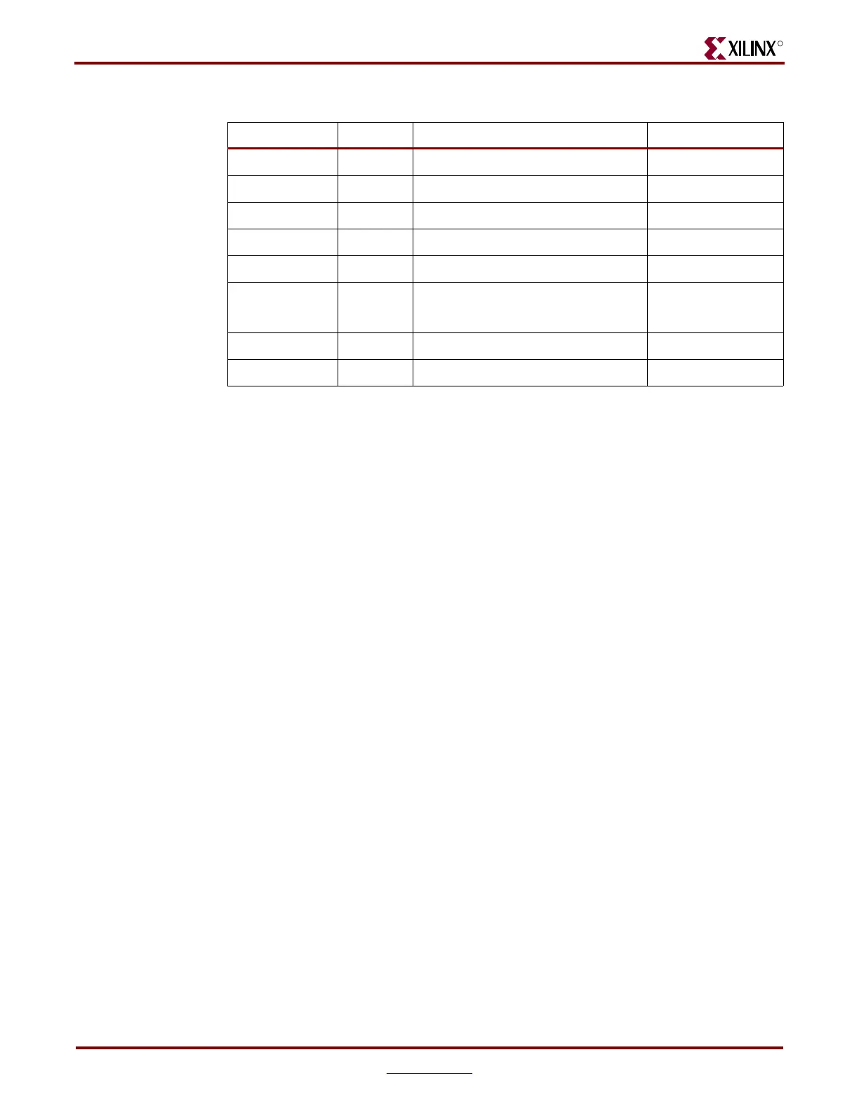
Table 6-3: Divider Settings
DADDR[15:0] DEC DI[15:0] Function
52h 0000 0000h (0000000000000000) N/A
52h 0001 0001h (0000000000000001) Divide by 2
52h 0002 0002h (0000000000000010) Divide by 3
52h 0003 0003h (0000000000000011) Divide by 4
52h 0004 0004h (0000000000000100) Divide by 5
•
•
•
•
•
•
•
•
•
•
•
•
52h 0030 001Eh (0000000000011110) Divide by 31
52h 0031 001Fh (0000000000011111) Divide by 32

 Loading...


