Virtex-4 FPGA Configuration User Guide www.xilinx.com 41
UG071 (v1.12) June 2, 2017
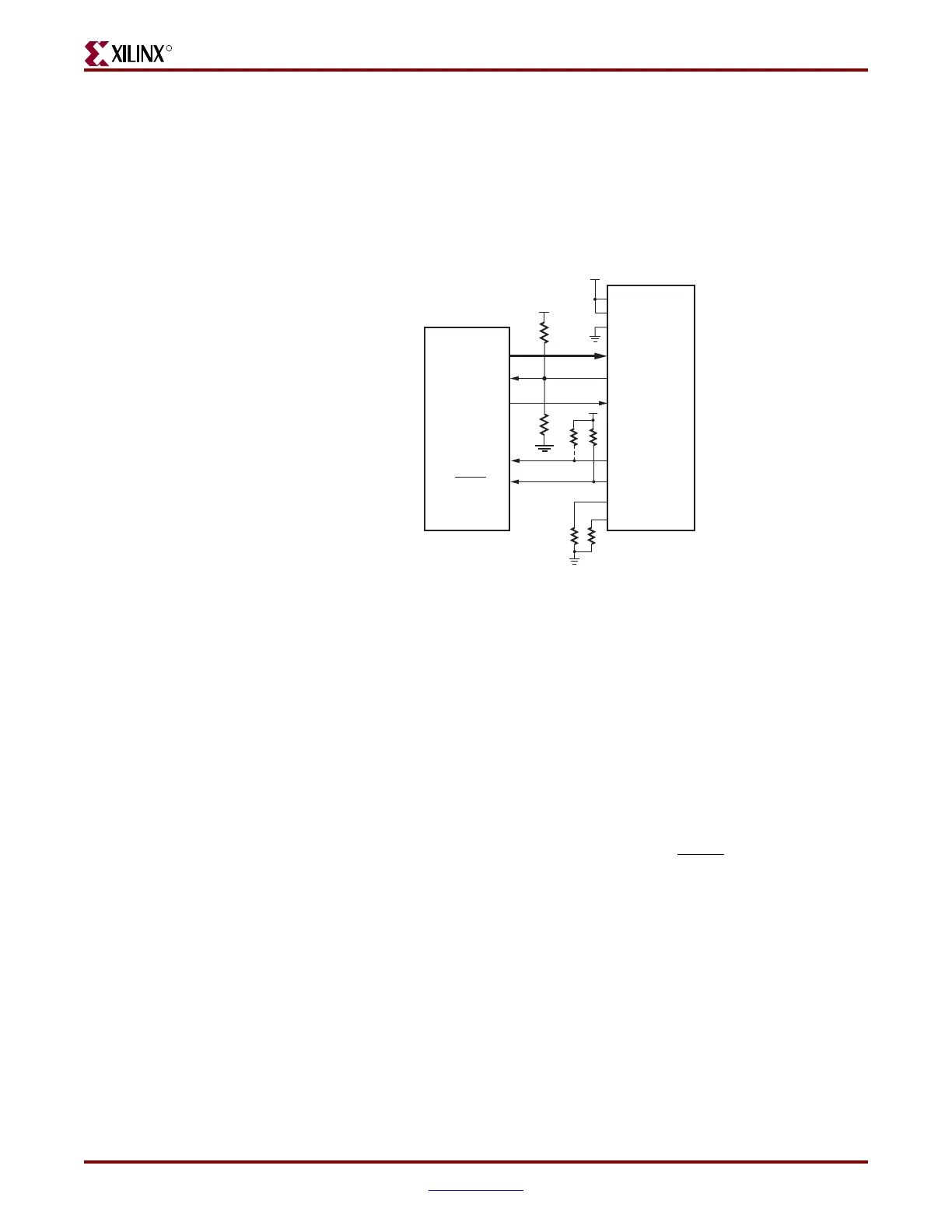
SelectMAP Configuration Interface
Single Device SelectMAP Configuration
The simplest way to configure a single device in SelectMAP mode is to connect it directly
to a parallel configuration PROM as shown in Figure 2-12. In this arrangement, the device
is set for Master SelectMAP mode, and the RDWR_B and CS_B pins are tied to Ground for
continuous data loading (see “SelectMAP Data Loading”).
Notes relevant to Figure 2-12:
1. The DONE pin is by default an open-drain output requiring an external pull-up
resistor. A 330Ω pull-up resistor is recommended. In this arrangement, the active
DONE driver can be enabled, eliminating the need for an external pull-up resistor.
2. The INIT_B pin is a bidirectional, open-drain pin. An external pull-up resistor is
required.
3. The BitGen startup clock setting must be set for CCLK for SelectMAP configuration.
4. The PROM in this diagram represents one or more Xilinx serial PROMs. Multiple serial
PROMs can be cascaded to increase the overall configuration storage capacity.
5. The .bit file must be reformatted into a PROM file before it can be stored on the serial
PROM. Refer to the “Generating PROM Files” section.
6. On XC17V00 devices, the reset polarity is programmable. RESET
should be set for
active Low when using an XC17V00 device in this setup.
7. The Xilinx PROM must be set for parallel mode. Note that this mode is not available
for all devices.
8. When configuring a Virtex-4 device in SelectMAP mode from a Xilinx configuration
PROM, the RDWR_B and CS_B signals can be tied Low (see “SelectMAP Data
Loading”).
9. The BUSY signal does not need to be monitored for this setup and can be left
unconnected (see “SelectMAP Data Loading”).
10. The CCLK net requires Thevenin parallel termination. See “Board Layout for
Configuration Clock (CCLK),” page 34.
11. The CCLK pin is an output and an input.
Figure 2-12: Single Device Master SelectMAP Configuration
ug071_22_073007
Virtex-4
Master
SelectMAP
D[0:7]
PROGRAM_B
CCLK
DONE
INIT_B
DATA[0:7]
CCLK
CF
CE
RDWR_B
CS_B
RESET/OE
Xilinx
Serial PROM
(2)(1)
M2
M1
M0
(10)
(10)

 Loading...


