34 www.xilinx.com Virtex-4 FPGA Configuration User Guide
UG071 (v1.12) June 2, 2017
Chapter 2: Configuration Interfaces
required. If additional time is required for the DONE signal to rise, the BitGen donepipe
option can be set for all devices in the serial daisy chain. (Refer to the BitGen section of the
Development System Reference Guide for software settings.)
Board Layout for Configuration Clock (CCLK)
The Virtex-4 output standard for all configuration I/Os, including CCLK, is different from
previous Xilinx FPGAs. To improve performance, the Virtex-4 configuration I/Os use the
LVCMOS fast slew rate standard of 12 mA. This change results in faster edge rates to
support higher configuration frequencies. This requires more attention to PCB trace
routing and termination for proper signal integrity.
These basic guidelines must be followed:
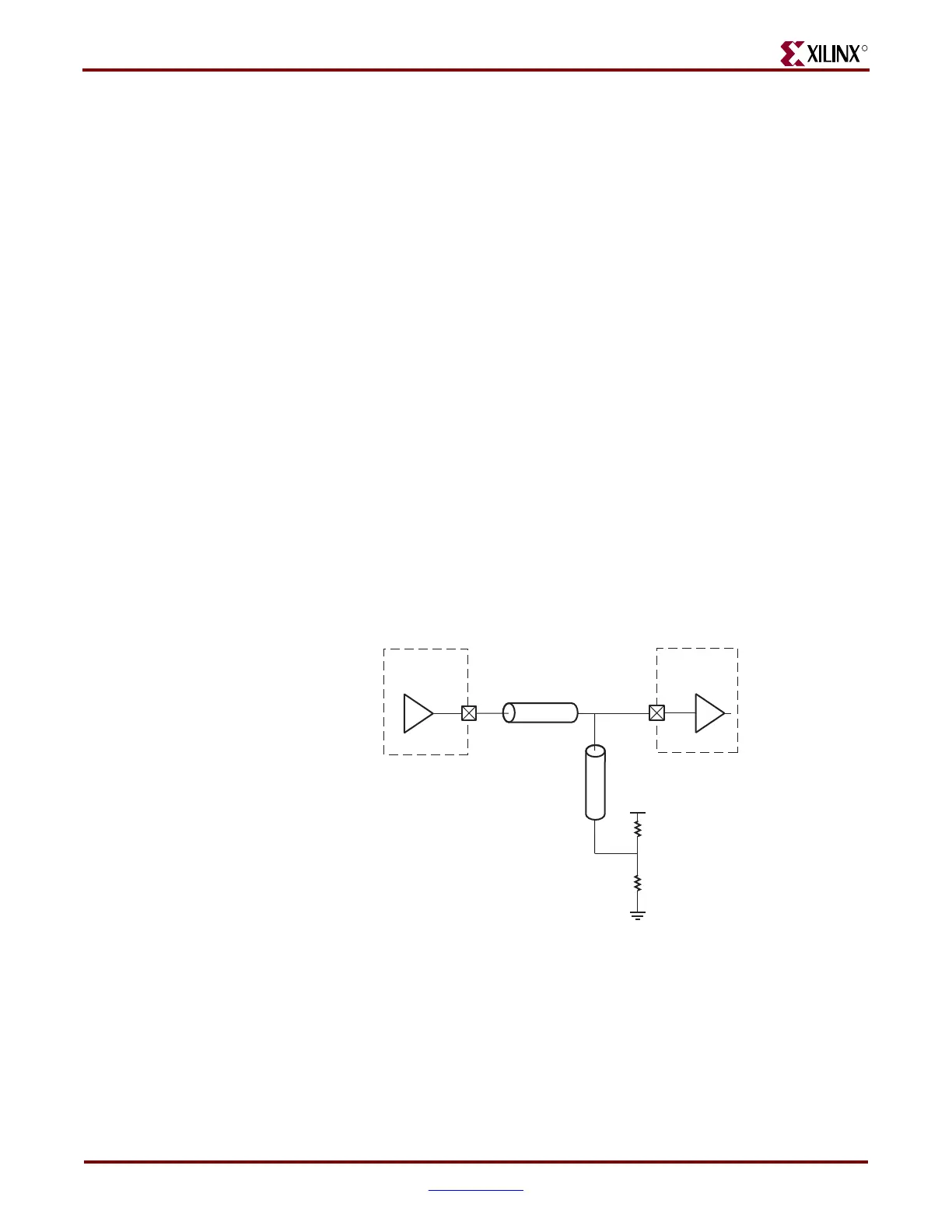
• Route the CCLK net as a 50Ω controlled impedance transmission line.
• Always route the CCLK net without any branching, do not use a star topology
(Figure 2-9).
• Stubs, if necessary, must be shorter than 8 mm (0.3 inches).
• Terminate the end of the CCLK transmission line with a parallel termination of 100Ω
to V
CCO
, and 100Ω to GND (the Thevenin equivalent of V
CCO
/2, and assuming a
trace characteristic impedance of 50Ω).
Xilinx recommends simulating the CCLK distribution with an IBIS simulator (such as
HyperLynx) to check for glitches on each CLK input, including the CCLK of the master
FPGA.
Figure 2-6 through Figure 2-8 show the recommended topologies for CCLK distribution.
Figure 2-6 shows the basic point-to-point topology for one CCLK driver (FPGA master)
and one CCLK receiver (PROM or FPGA slave).
Figure 2-6: Point-to-Point: One CCLK Output, One CCLK Input
CCLK Output = Master FPGA
CCLK Input = PROM or Slave FPGA
CCLK
Output
ug071_2_06_072505
Z
0
(50 Ω)
CCLK
Input
Z
0
(50 Ω)
2 x Z
0
(100 Ω)
2 x Z
0
(100 Ω)
V
CCO_0

 Loading...


