Virtex-4 FPGA Configuration User Guide www.xilinx.com 15
UG071 (v1.12) June 2, 2017
Setup (Steps 1-3)
Setup (Steps 1-3)
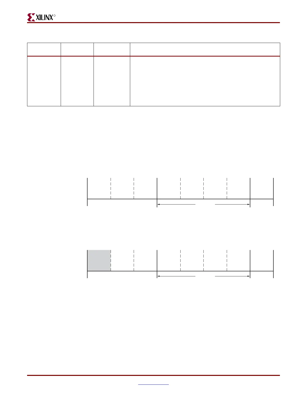
While each of the configuration interfaces is different, the basic steps for configuring a
Virtex-4 device are the same for all modes. Figure 1-1 shows the Virtex-4 configuration
process. Each step is described in detail in the following sections.
Device Power-Up (Step 1)
For configuration, Virtex-4 devices require power on the V
CC_CONFIG
, V
CCAUX
, and
V
CCINT
pins. There are no power-supply sequencing requirements.
All JTAG and serial configuration pins are located in a separate, dedicated bank with a
dedicated V
CC_CONFIG
(V
CCO_0
) supply. The SelectMAP data pins are shared dual-
purpose pins, and are located in Bank 2 (V
CCO_2
). All dedicated input pins operate at
V
CC_CONFIG
LVCMOS level. All active dedicated output pins operate at the V
CC_CONFIG
voltage level with the output standard set to LVCMOS_12F. In SelectMAP mode, V
CCO_2
must be connected to the appropriate voltage to match the I/O standard of the
configuration device.
HSWAPEN Input Dedicated Active High input used to disable weak pre-configuration I/O pull-up
resistors:
0 = weak pre-configuration I/O pull-up resistors enabled
1 = weak pre-configuration I/O pull-up resistors disabled
HSWAPEN must be connected to either enable or disable the pull-up
resistors.
HSWAPEN has a weak pull-up prior to and during configuration. The
weak pull-up does not always provide a reliable 1.
Notes:
1. The Bidirectional type describes a pin that is bidirectional under all conditions. If the pin is an input for some configuration modes or an
output for others, it is listed as an Input or Output type.
2. Dual-purpose pins can become user I/O after configuration. See “
PERSIST” in Chapter 7 for details.
Table 1-2: Virtex-4 Configuration Pins (Continued)
Pin Name Type
(1)
Dedicated or
Dual-Purpose
(2)
Description
Figure 1-1: Virtex-4 Configuration Process
Device
Power-Up
Sample Mode
Pins
Synchronization
Device ID
Check
CRC Check
Clear
Configuration
Memory
Startup
Sequence
Load
Configuration
Data
Start
Finish
Bitstream
Loading
ug071_01_122105
Steps
12345678
Figure 1-2: Device Power-Up (Step 1)
Device
Power-Up
Sample Mode
Pins
Synchronization
Device ID
Check
CRC Check
Clear
Configuration
Memory
Startup
Sequence
Load
Configuration
Data
Start
Finish
ug071_02_122105
Bitstream
Loading
Steps
12345678

 Loading...


