80 www.xilinx.com Virtex-4 FPGA Configuration User Guide
UG071 (v1.12) June 2, 2017
Chapter 6: Reconfiguration Techniques
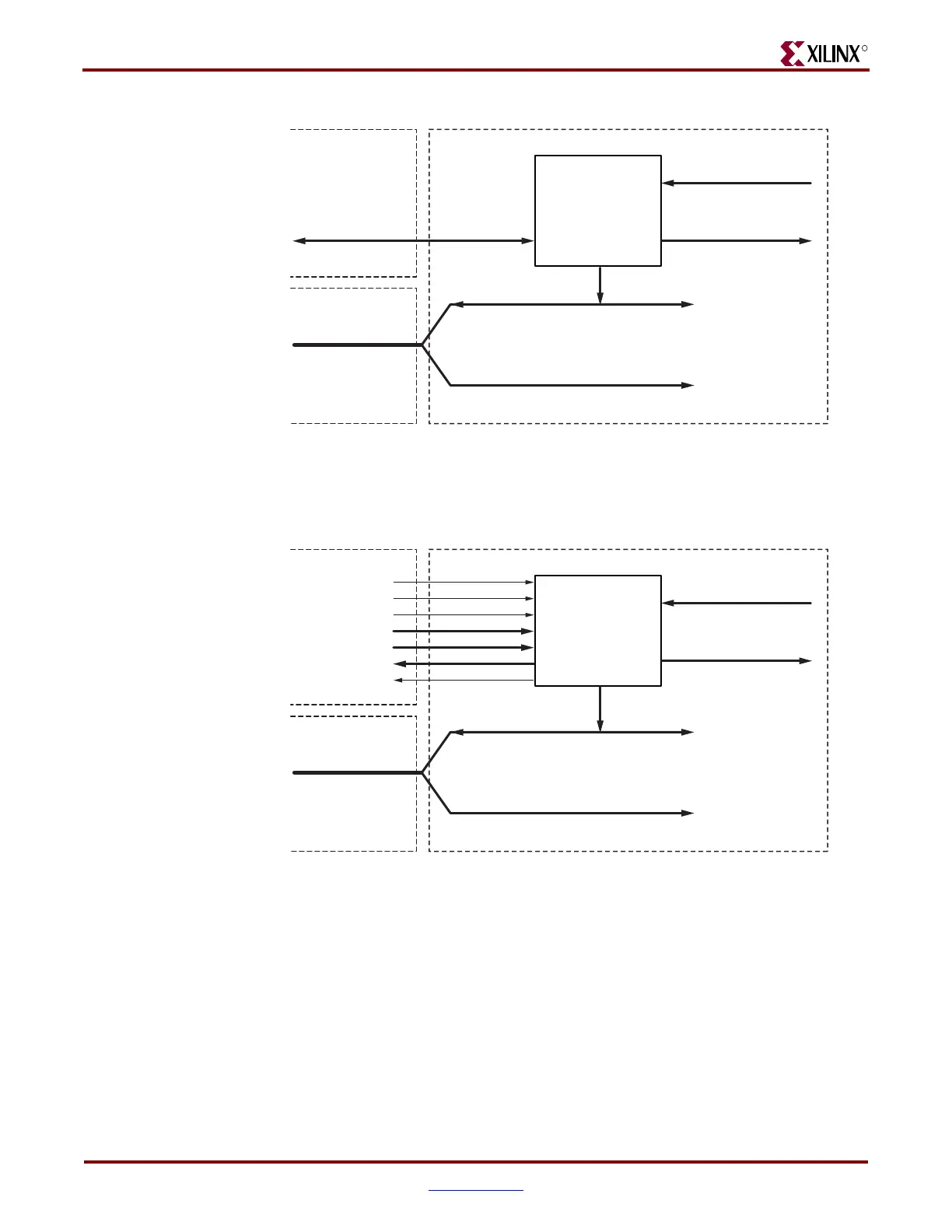
Figure 6-3 is the same as Figure 6-2, except the port between the Logic Plane and
Functional Block is expanded to show the actual signal names and directions.
FPGA Fabric Port Definition
Table 6-1, page 82, lists each signal on the FPGA Fabric port. The individual functional
blocks can implement all or only a subset of these signals. The DCM chapter in the
Virtex-4 FPGA User Guide and the Virtex-4 RocketIO Multi-Gigabit Transceiver User Guide
shows the signals and functions implemented for the specific blocks. In general, the port is
a synchronous parallel memory port, with separate read and write buses similar to the
block RAM interface. Bus bits are numbered least-significant to most-significant, starting
at 0. All signals are active High.
Figure 6-2: Block Configuration Logic with Dynamic Interface
Figure 6-3: Block Configuration Logic Expanded to Show Signal Names
CONTROLLER
Block Status
(Read-Only Ports)
Function Enables
(Write-Only Ports)
Reconfigurable Bits
All configuration bits
for this block
Non-reconfigurable Bits
to block logic
to block logic
Standard
Reconfiguration
Port (to fabric)
Configuration Logic Functional Block (DCM or MGT)
Logic Plane
ds071_42_071705
CONTROLLER
Block Status
(Read-Only Ports)
Function Enables
(Write-Only Ports)
Reconfigurable Bits
All configuration bits
for this block
Non-reconfigurable Bits
to block logic
to block logic
Standard
Reconfiguration
Port (to fabric)
Configuration Logic Functional Block (DCM or MGT)
Logic Plane
ds071_43_071705
DCLK
DRDY
DEN
DWE
DADDR[m:0]
DI[n:0]
DO[n:0]

 Loading...


